Atari 1050 Disk Drive with Capacitor Troubles

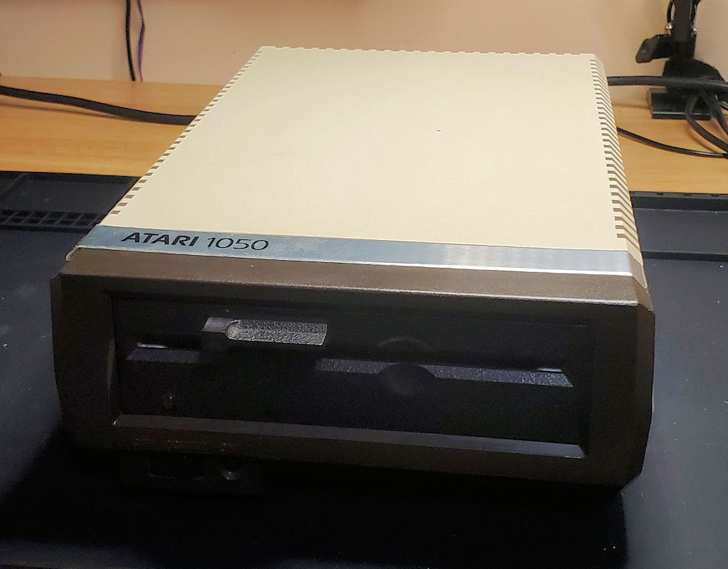
As part of a bulk purchase of Atari related items I had done, was an Atari 1050 Disk Drive.  Of course, with any vintage hardware one might acquire, it is good practice to inspect such devices before applying power to said device.  In my inspection of the Atari 1050 disk drive, there was a distinct rattling sound of which I knew was not a feature of this device in its original configuration.  So, it was time to pull out my screwdriver and open it up to see what all this noise was about.

For those who don’t know, (which might include some of my family members) the Atari 1050 disk drive is a 5.25-inch floppy disk drive manufactured by Atari in the 1980’s.  It is used for data storage on the Atari 8-bit computers.

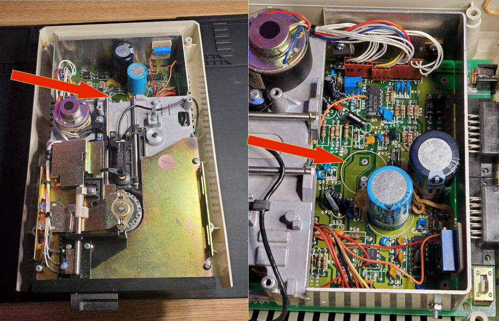
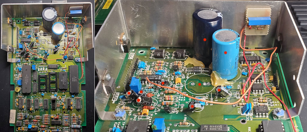
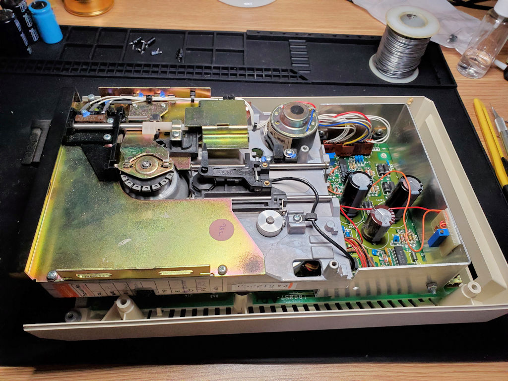
Upon removing the screws and removing the top of the case, it became clear that the rattling noise I heard came from a capacitor bouncing about loose inside the unit.  This is not the normal way a capacitor works so it’s clear I have some repair work to do before we get to power this unit up just to see if there are any other issues to be addressed.

The arrows above point to the spot where a capacitor should be.  Also, if you look closely at the view on the right you can see what looks to be the remains of a rubber-band.  And furthermore, it almost looks like someone attempted to put some glue or epoxy between the missing capacitor and the light blue capacitor just in front of it.  I’m really not sure what was trying to be accomplished here, but whatever it was looks to be an epic fail in my opinion.  You can also see a hardware modification which we will get to in a bit.

The Capacitor

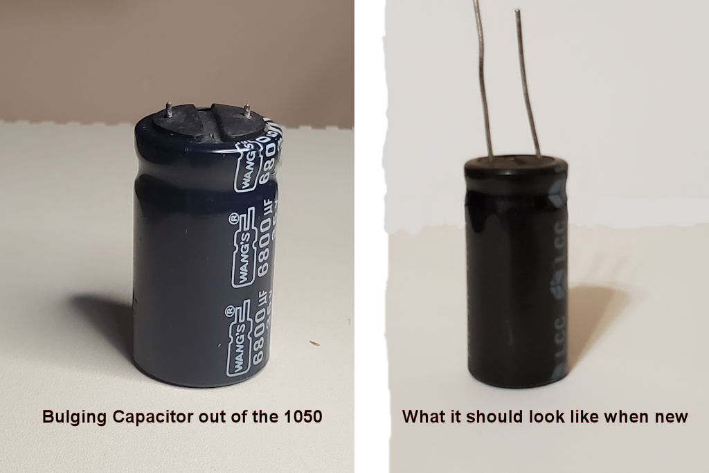
Okay, this is a first for me, I’ve seen leaking capacitors, and even bulging capacitors, but this is the first time I’ve found a bulging capacitor from the bottom in such a way that it literally popped the capacitor out of its socket.  Admittedly the solder joints for the capacitor are forty years old but I still found it interesting to see.  What this means is that I will replace all the electrolytic capacitors in this disk drive before we power it up.

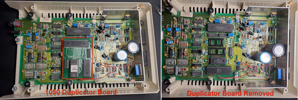
As I alluded to previously, during the inspection of the unit I clearly saw a modification that had been made to this unit.  This 1050 was modified with the 1050 Duplicator from Duplicating Technologies Inc.  As best I understand, this upgrade worked much like the Happy Computer enhancement that allowed for creating backups from copy protected disks.  However, based on what documentation I’ve found thus far, the 1050 Duplicator attempted to remove the copy protection and make your backup disks non-protected which would allow you to simply copy the non-protected disks as often as you like and would work with any disk drive.  Clearly this did not make the developers of such copy protected software happy.  It also provided via the hardware, faster read/write speeds and double density disk capabilities.

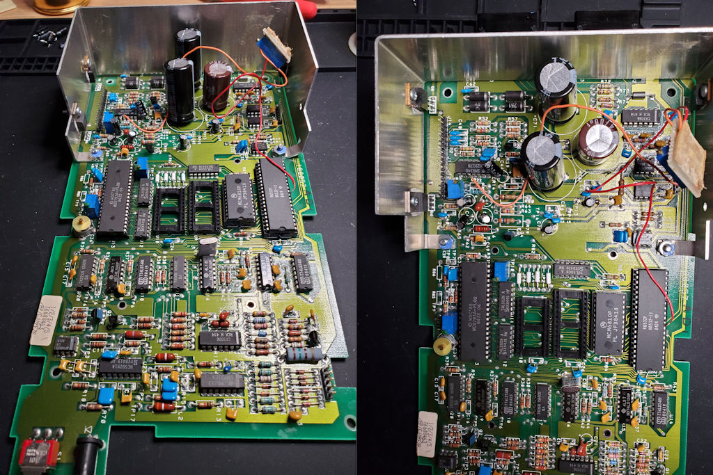
If I were to guess, those blobs next to the big capacitors is hot-gun glue.  Could it be they wanted to make the capacitors more secure on the board?   Still don’t know what the rubber-band is all about.

Back to my thoughts on the 1050 Duplicator.  Attached to the large aluminum heatsink there is a small board with a blue component.  I am guessing that this is some sort of Cermet Trimmer resistor as it does have an adjustment screw.  The board is attached by double sided tape which has long since dried out and this board will easily fall out of place.  So, as I confirmed the falling out of place bit, I did see there are a couple other components on the board under that tape.  And as the picture shows there are a couple of wires that run to their respective IC chip pins.   I don’t have the details of what this does, or if it is part of the 1050 Duplicator.  I can only assume (and we all know what that means) that since the original owner of this drive had this upgrade installed via a professional service, that it is part of the 1050 Duplicator system.

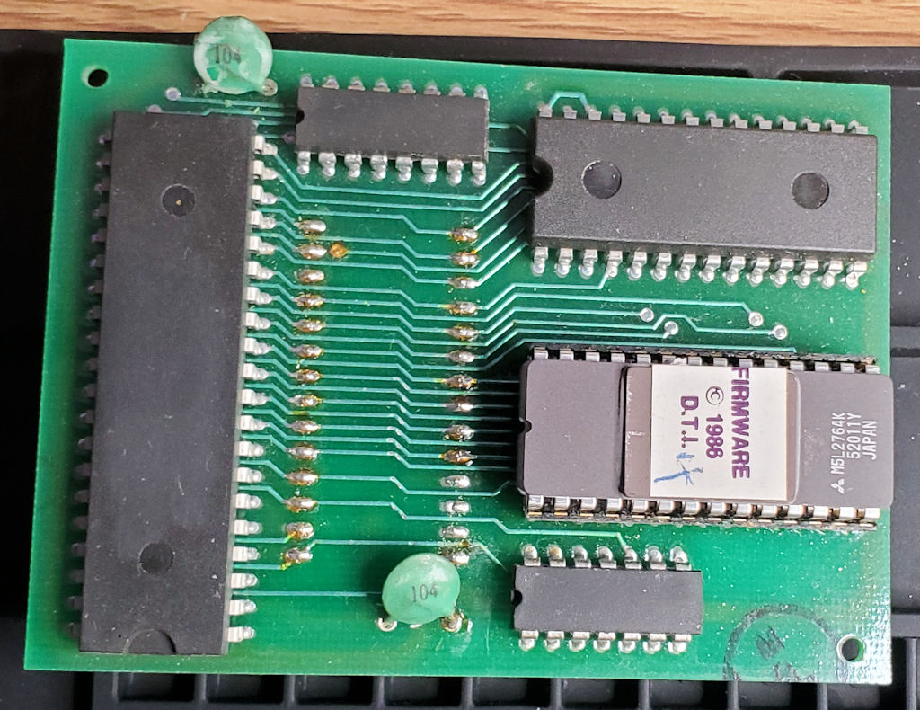
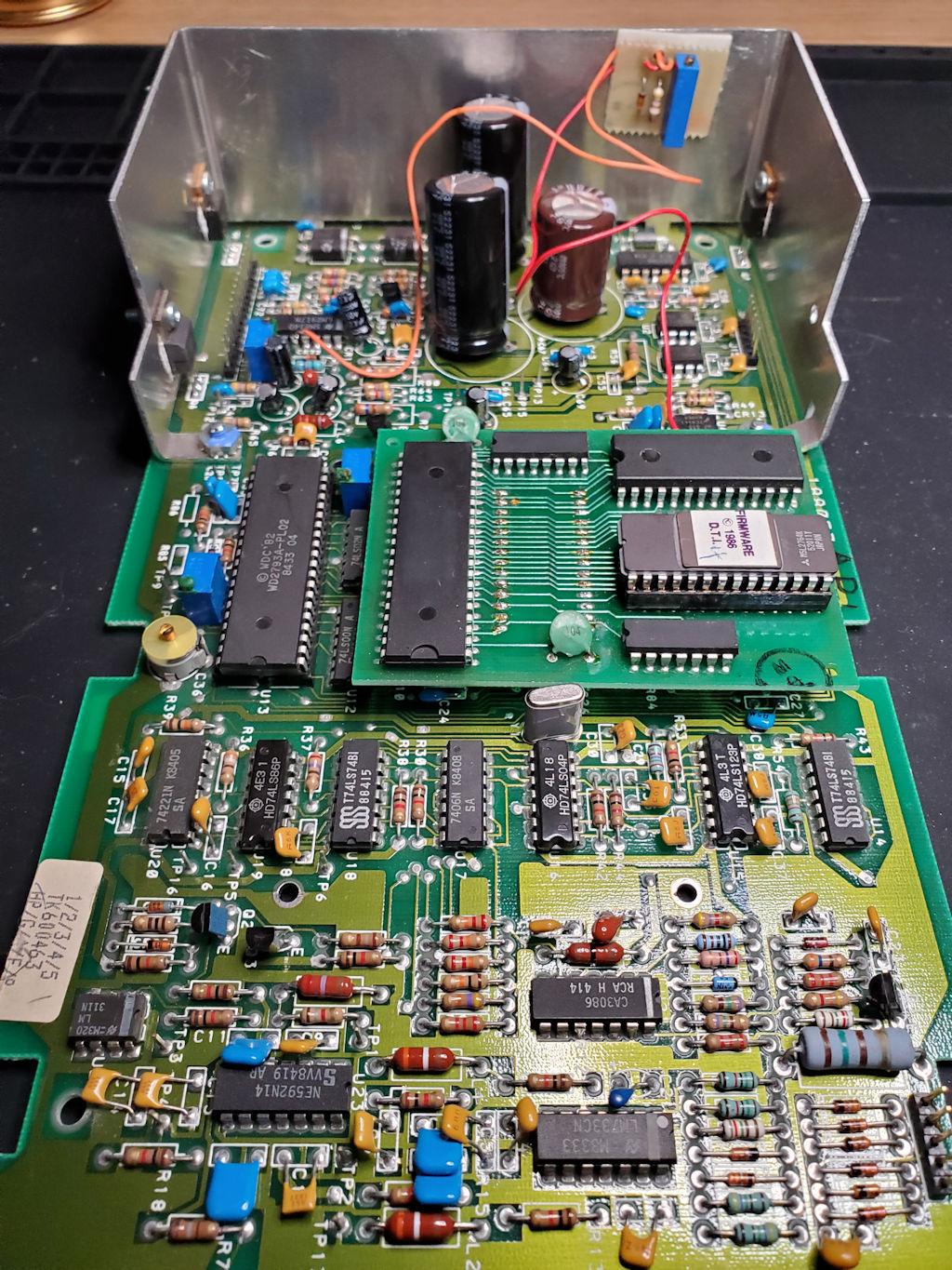
This is a closeup of the 1050 Duplicator board.  Notice that Duplicating Technologies was very good at removing any identifying information regarding the IC Chips they used on the board.   Other than their firmware EPROM, it is anybody’s guess on what these other chips do.   I suppose DTI could have done a bit better job cleaning up the solder flux on the socket header pins. 😊  And that 104 capacitor at the top looks a bit suspect.  I might have to think about replacing it if things don’t work so well after almost forty years.

Okay, enough of my rambling about what all this stuff is and on to the real task at hand which is replacing the electrolytic capacitors on the board.  A relatively simple task that requires little conversation so I will just show a few pictures of it instead.  This approach requires less reading on your part and less typing on mine.

With the disk drive mainboard out of the enclosure we will begin the capacitor replacement.  The nine points dotted in RED are the capacitors we will replace.  Note the missing capacitor point dotted has 3 thru-hole solder pads.  This is to accommodate capacitors with different leg spacing distance.  We will take advantage of this as my capacitors that will be replacing these old ones have the shorter leg distance.  And while I’m at it I will clean up that glue glob.

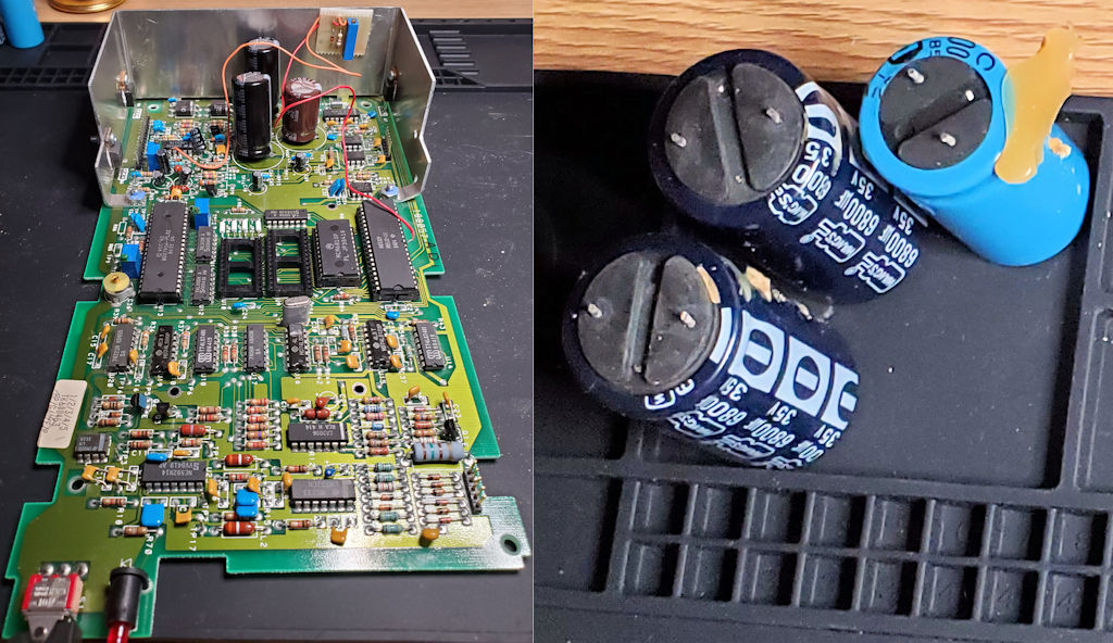
All electrolytic capacitors have been replaced.  Notice that the three large capacitors originally installed are replaced with physically smaller capacitors but have the same specifications as the OEM parts.

Left is the 1050 mainboard recapped and the 1050 daughter board taped back to the heatsink.  Right are the three old large capacitors removed and notice the other 6800uf capacitor was beginning to bulge on the bottom as well.   Would not have been long before it popped off the mainboard.  Actually, removing it was very easy and I most likely did not need to use my soldering iron to loosen it up for extraction.

Next is to plug in the 1050 Duplicator board and reassemble the disk drive for testing.

Okay, I’ve reassembled the disk drive and have everything plugged in.  I’ve left the top cover off so that I can make any adjustments necessary when testing.

The initial tests went well and I’m able to boot from the drive, write to disks, format disks in both single and double density.  There are moments where the drive seems to pause during I/O but does not happen all the time.  It may be something with how the 1050 duplicator board handles the I/O process.  It definitely tries to read and write data at higher speeds at all times.  I’m not sure if there are any settings I can change on this and will need to learn more about this upgrade to determine if I have issues, or just need to configure it to work in a particular way.

All in all, this drive is functional and ready to start storing data.

Building My Atari Cheep Talk

Atari Cheep Talk – Analog Magazine, Issue 29, April 1985

In the Analog magazine April 1985 issue there is an article on page 59 titled "Cheep Talk: Build your own speech synthesizer” by Lee Brilliant. Back then, I did not have the money or patience to build this “Cheep Talk” device but was fascinated by the article. So, I Xeroxed the article and stored it in one of my paper binders. I must have borrowed the magazine from someone else as I never had a subscription to Analog, or recall purchasing this issue.

Recently, I was perusing through one of my binders and ran across the article. Today you can read all the Analog magazines as they are freely available on Atarimania, or the Internet Archives, amongst other places. As such, I jumped on over to Atarimania and looked up the issue in question and decided to attempt to build this Cheep Talk device that eluded me back in 1985. What follows is my attempt at constructing this device just as described in the article.

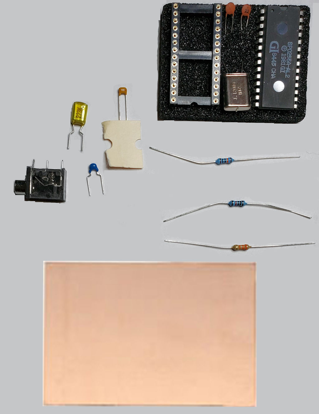
My first objective is to acquire the parts needed to construct this device. The main component that is needed is no longer manufactured as it is a Radio Shack (General Instruments) SP0256-AL2 speech chip. You can still find these on eBay as New Old Stock (NOS) and I picked one up for $57 which also includes two 22pf capacitors, one precision IC socket (nice touch), and one 3.12MHz crystal which is the original crystal planned for use by the author at that time but was substituted by his parts list. All the other components are readily available from places such as DigiKey, or Jameco. And since I stated I was constructing this project just as was from the magazine article, needed to get a single sided copper clad breadboard that I will use to make the circuit board.

Cheep Talk Components

I will provide the full list of the components needed/used at the end of this post, but to summarize, it is 3 resistors, 5 capacitors, 1 crystal, the SP0256-AL2 Speech Synthesizer IC, and the PCB. To make this functional beyond the electrical components will also need 2 DB9 serial connectors and an amplified speaker of some sort.


Circuit Board Construction

It has been 25+ years since I did anything with PCB etching and technology has really changed for the design process. The home DIY boards made from back in the 80’s from when I learned to do this would make use of etchant resist pens (Sharpie’s) and rub on transfer tape that would cover the copper with your circuit design. Today the expectation is that you build your circuit in one of the many CAD programs available and then transfer that circuit to the PCB via printout using a hot or cold printer toner method, or by use of photo developed PCB method. Rub-on circuit transfer tape is no longer manufactured and of course you can still use the Sharpie method, but still must deal with the flaws of this approach.

For my first attempt I opted for the Hot transfer toner method. Since the circuit design is provided in the magazine article, I only need to print it out in mirrored format on glossy magazine paper (cheap way to do it), or on vinyl print paper which allows for better visual of the circuit printed as you don’t need to read thru the already printed text/graphics of magazine paper. As my vinyl print paper had yet to arrive, I decided to give this magazine paper a try.

As mentioned above I’m doing the Hot transfer method (toner) which requires that we first print the circuit to be transferred to the PCB via a laser printer. Inkjets will not work for this approach as it is the toner of the laser printer that will be deposited to the copper of the PCB from the paper. Keep in mind that you need to scale the printout to match the actual size of the circuit traces intended. This is critically important for IC socket connections as pin location needs to be accurate.

An issue brought up for the above method(s) is that the Brother Laser printer(s) of which I own do not do a good job of toner distribution for this application. I can confirm that in my case this is true. I don’t think it is the toner distribution as much as it is how the Brother technology deposits toner on print medium. So, it may not really matter if you are using OEM Brother toner cartridges, or a generic brand. In any case, the printout was not of high quality.

The next step in this process is to take your circuit printout and position it print side down on the copper PCB of which you will want to etch the circuit. Next you get your trusty clothes iron, you know the one that has been sitting in the closet (or in my case the garage) the last 10 years collecting dust and put the heat setting to around 170 degrees. I got my digital thermometer out just to be as accurate as possible. You then start ironing on the PCB for 5 to 7 minutes. It is a good idea to put a cloth of some sort over the print medium you are using as we really are not looking to start a fire. We just want to use heat and pressure to deposit the toner from the paper on the copper of the PCB. Once done, let the PCB cool off for a few minutes.

Now we carefully peel back and remove the print medium from the PCB and if all went well the toner has adhered to the copper of the PCB forming your circuit trace. In my first try it looked to have done a fair job, but I did have to go over most of the traces with a Sharpie as there was copper still visible in many locations of the circuit trace. I let the Sharpie ink dry for about an hour and then attempted my first etching. I’m still using the tried-and-true Ferric Chloride solution and about 15 minutes later had to take the PCB out of the solution and rinse off.

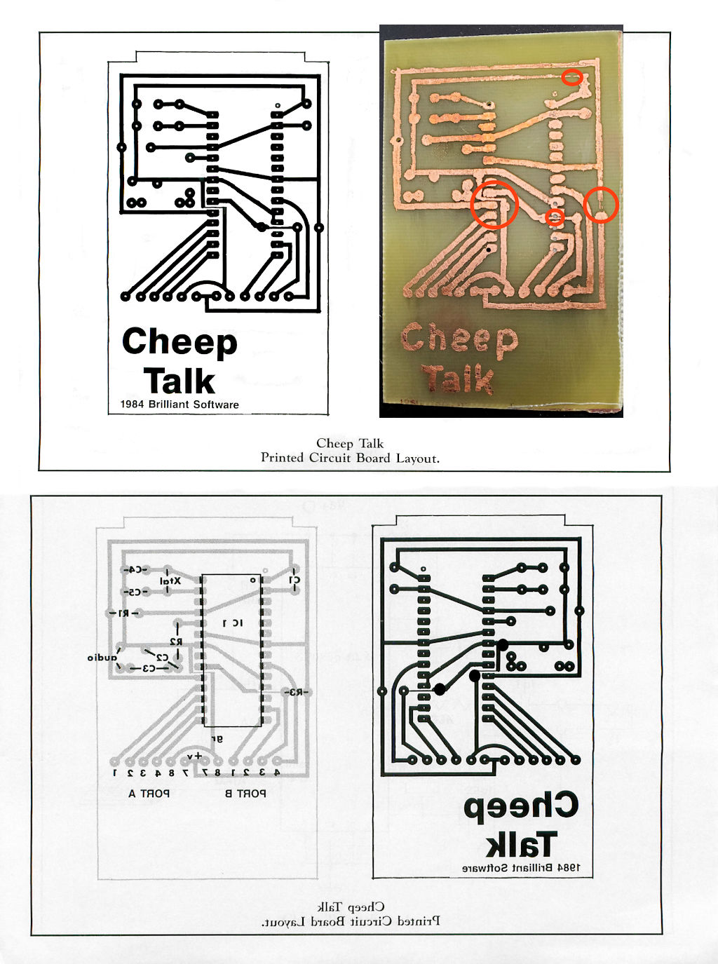
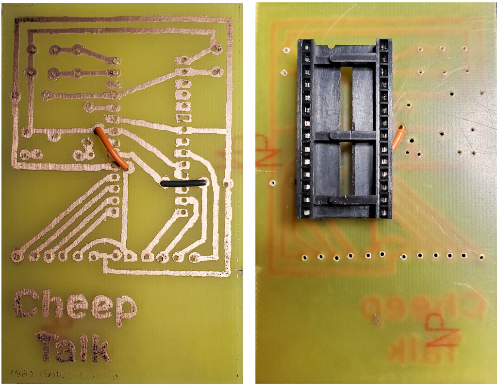
The above picture shows the circuit diagram from the magazine article and my first run of the PCB etch.  I circled all the issues in RED for the PCB.

  • The most challenging issue is with etching away too much of the copper as you can see the circuit trace has a gap. This was always a concern when you did not have enough coverage with the etch resist pen and/or transfer tape years ago.  It makes timing crucial of the etching process to remove all the exposed copper, but not what you traced on the board.
  • The next issue of which I noticed and attempted to plan for is two circuit traces going in between the IC socket solder pads. For the home DIY’r that’s a really fine line needing to be etched.  I had planned for this and added solder pads to the circuit with the expectation that I would use jumper wire to address this challenge.  Also, these circuit traces are so close to the IC socket solder pads, chances are very high I would have solder jumping over on to the circuit trace and shorting it out.
  • And of course, with the DIY approach of using etch resist pens and my Brother laser printer, my circuit traces are far from precision. But this first attempt let me work out how to drill the holes in this board.  You can see where I misaligned an IC socket template I used on this board and ended up drilling off center and through circuit traces.

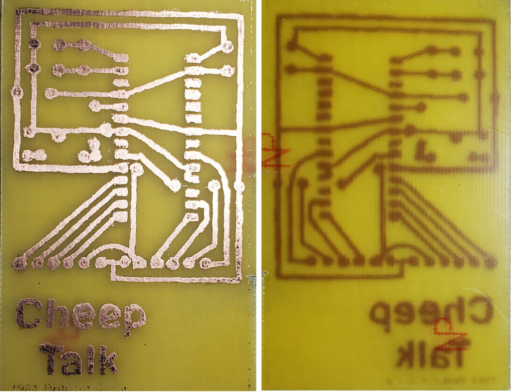
My second attempt at etching this board went better.  I used the same Hot Transfer method as my first attempt but with vinyl print paper as the medium to deposit the toner.  It is clear that the Brother laser printer is not very useful for toner transfer PCB projects.  I did have to do a lot of touch up work to the board with a Sharpie prior to etching.

I did find that removing excess toner from the board takes more work than the Sharpie solution.  Steel wool or 3M green scrubbing pads are needed.  Not a big deal, just more effort than acetone cleanup.  I was satisfied with this attempt and used an X-acto knife to address any residual copper tracings left on the board.  Next step is to drill the holes in this.

For this board I removed the circuit traces between the IC socket connections in favor of using a jumper wire to complete those two circuit traces.  The above photo shows them on the bottom of the board for placement, but I will be installing them on the top of the board.  I also decided to use an IC socket with long legs as it provides me clearance to connect the jumper wires on the top of the board and makes it a bit easier to insert the socket in the board as my drilling of holes is not as perfectly aligned as a commercial machine drilled holes.


Installing the Components

My first step was to test fit the components and right off I found that I had forgot to provide a solder pad for one of the jumper wires which was meant to be used for a resistor.  In this case I will drill another small hole right next to the solder pad where I can route the resistor wire through to tie into the solder pad.  A little more solder to flow over and connect the pad will work if not the prettiest solder joint.

With that SNAFU fixed up the rest of the component placement went as planned.  Now on to soldering in place.

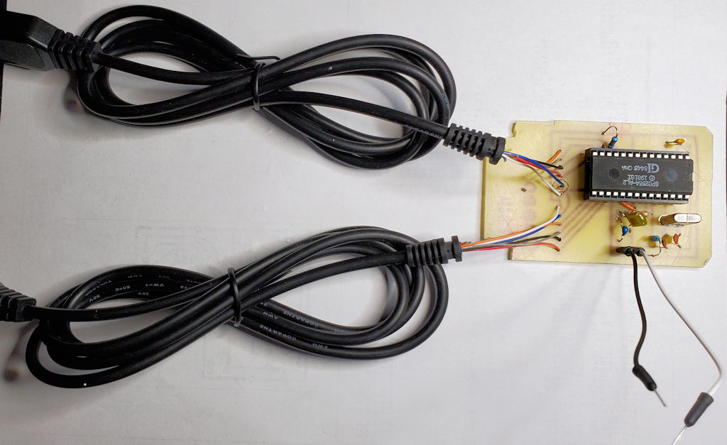
If you look closely you can see where I installed the gray and orange jumper wire on the board through the IC socket pins.  The black markings on the edge of the PCB are where I need to cut away to allow for proper fit inside the project case I have.  The open holes on the board will be for the two joystick cables and speaker jack.

In the article the author notes that he used an external amplified speaker for the project and cautioned that hooking up to a stereo amplifier could damage the Cheep Talk or your Atari if the amplifier generates additional voltage on inputs you may decide to use.  As such he recommends using one of Radio Shack’s small, amplified speaker units.  My initial plan was to use one of the many small computer speaker sets in my inventory from years in the PC industry.  But then noticed the author also stating that you could use the cassette audio output/input pin 11 on the SIO jack of the Atari and let it play through your TV speakers.  And the article further notes that in doing so you only need to use one wire for this as the Cheep Talk circuit is already grounded through the Joystick port cabling eliminating the need for an external ground source of an amplified speaker unit.  Upon reading this tidbit of information, I elected to take this approach as I am already hooking up to a TV and will have an open SIO port that I can connect to pin 11 of.  Besides, I have many Dupont wires laying about that will fit nicely into both devices.

Another change I made was to use standard 9 pin molded Joystick cables as opposed to ribbon cable the author used.  Looks much more professional in my opinion.

Putting Cheep Talk In The Project Enclosure

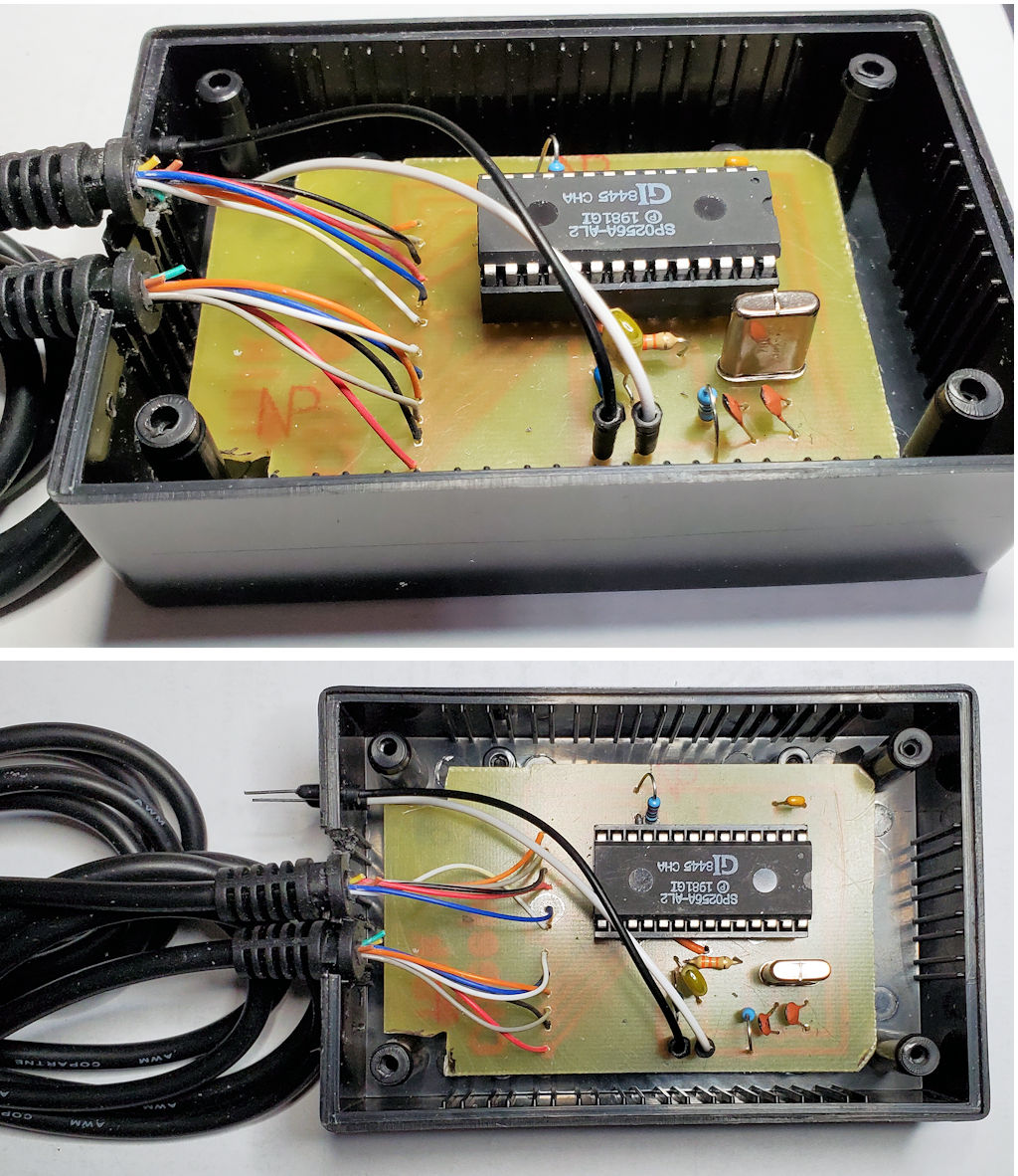
Now that I have finished all the solder work and cleaned up the board, it is time to put it in the project box after doing a little construction work to said enclosure.  I needed to cut openings for the cable strain relief plugs and holes for the speaker connection(s).  At this point I’m going to leave both connection wires in place should I decide at a future date to connect an external speaker of some sort.  It does have to be an amplified (powered) speaker as the Cheep Talk device provides no speaker amplification.   This is where the benefit of using pin 11 on the Atari SIO jack makes sense as your TV already has amplified speakers that the audio generated by Cheep Talk flows.

The PCB will be secured to the case with two small panhead screws of which the lip of the screwhead will hold it tight to the enclosure bottom.  This way I don’t need to do any more drill holes in the board.  Also, the black wire extending out to external connection point is what I use for the audio output to the TV.  The white wire is technically a grounding circuit and would be used with an external amplified speaker solution along with the black wire should I ever decide to use it.

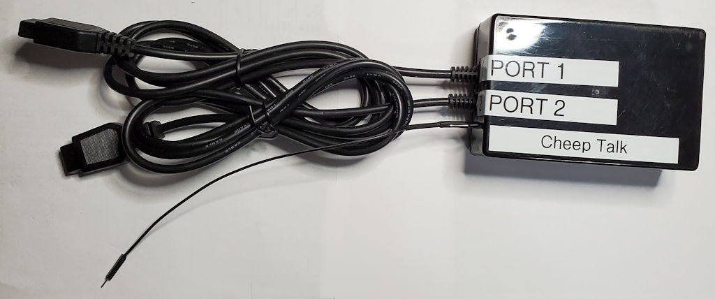
This is the completed Cheep Talk device I built.  Requires the use of both joystick ports on the XL/XE computers and being connected to an amplified speaker source.  Power for the device is provided by the joystick port(s).

Project Takeaways

I’m quite proud of my work on this project.  It turned out fully functional and looks good in the case I had on hand.

  • Okay, this has inspired me to dig deeper of the new PCB fabrication being done today. Still like the ferric chloride etching approach but need to up my skills on how we design and prep PCB’s for etching.
  • Some may say that what this device does is no different than S.A.M. (Software Automated Mouth), a program for the Atari that does the same thing. However, a key difference is that all the processing for the speech is done on the device allowing the computer to work on the programming more efficiently as it does not need to allocate precious resources to the actual speech processing.

Just a fun project overall even though Amazon Alexa’s speech processing is light years better.  Now its on to learning how to program this thing to do more then the sample programs provided in the article.

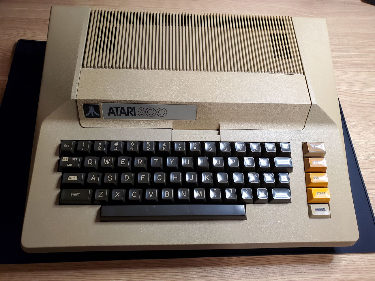
Atari 800 Keyboard Restoration

The Atari 800 is the computer which I first saw my brother David use that inspired me to jump on to the Atari bandwagon back in the 80’s if memory serves.

I picked up my Atari 800 sometime in the late 90’s I think, and never really did much with it as I already was using my 800XL and 65XE computers.  So, it with other Atari computers I’ve collected sat on a shelf in my closet for years.  During the 2020 pandemic lockdown, I had time to pull all my Atari computers and peripherals out of storage and test their workings, and to my surprise, the 800 powered up without any issues but one…

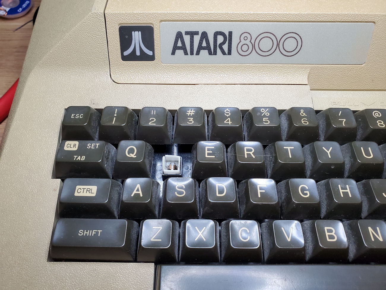
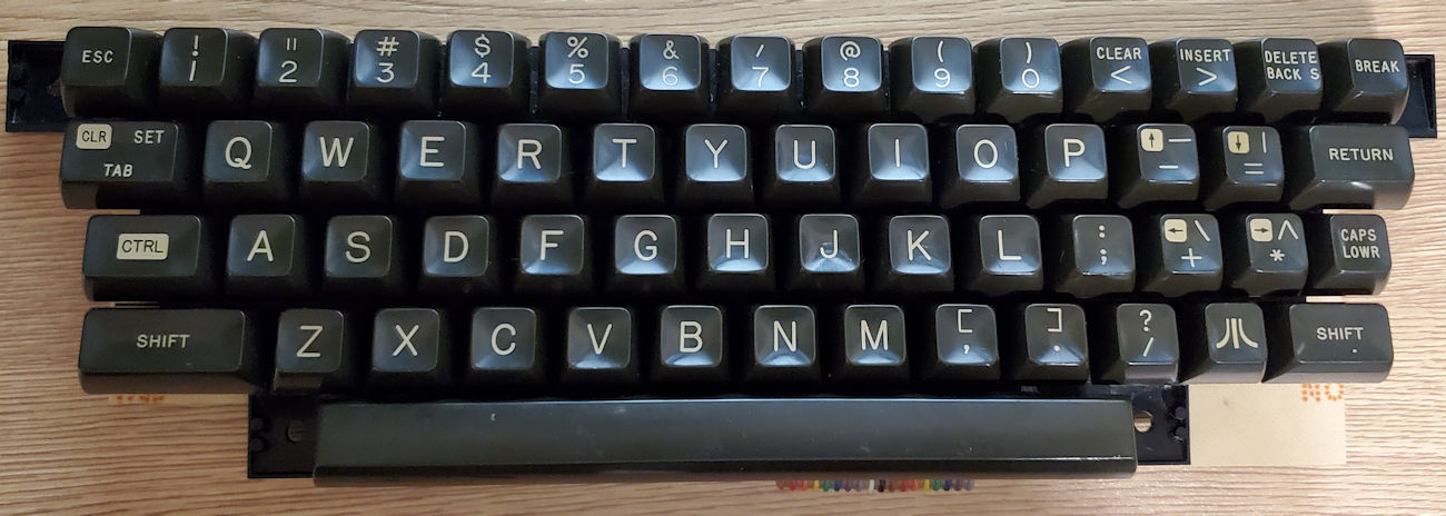
A common problem for many of the Atari 800 computers with the mechanical keyboard is the keys binding up and sticking when attempting to type.  The issue has to do with the key sleeves splitting at the corners.  Some keys such as the QWERTY row were more likely to bind and stick down when pressed just due to the angle of your keystroke.  As such, I really couldn’t use the keyboard on this computer for any serious typing, and at forty plus years old, there are no replacement keyboards available.

Then as I was reading my social media Atari group feeds, I came across some other users that implemented a solution via the help of a 3D printer to fix their 800 keyboard woes much the same as mine.  You gotta love technology of today that fixes issues with that old technology you grew up with.  And for $20 an industrious individual printed a solution for my keyboard woes.  Below I walk through the solution implemented to fix my keyboard.

The Atari 800 is a handsome looking machine even by today’s standards.  The keyboard was much like an electric typewriter of the day and was/is a pleasure to type with.  This particular Atari 800 has the Hi-Tek mechanical keyboard.  There was also a Mitsumi mylar based keyboard used with the 800 in other production units.

For this repair, we will need the 3D printed collars and some UV activated superglue.  You will see in the upcoming photos how the 3D printed collars provide the fix for this keyboard.

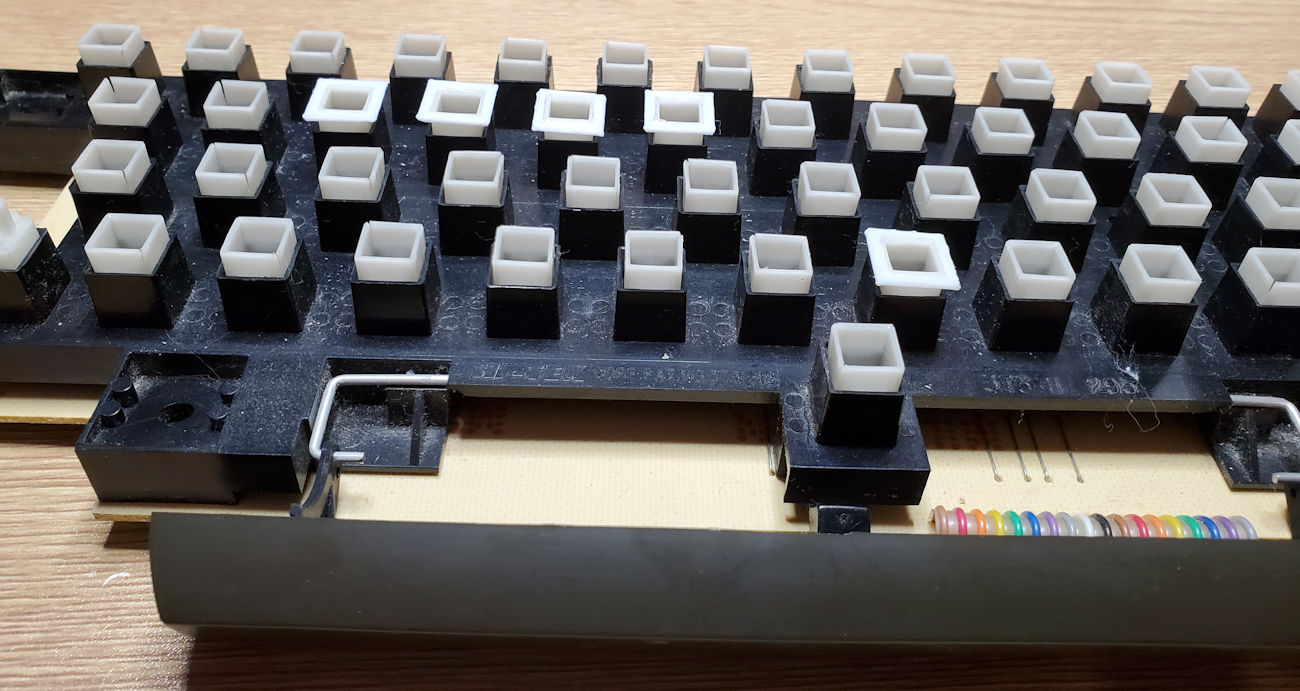
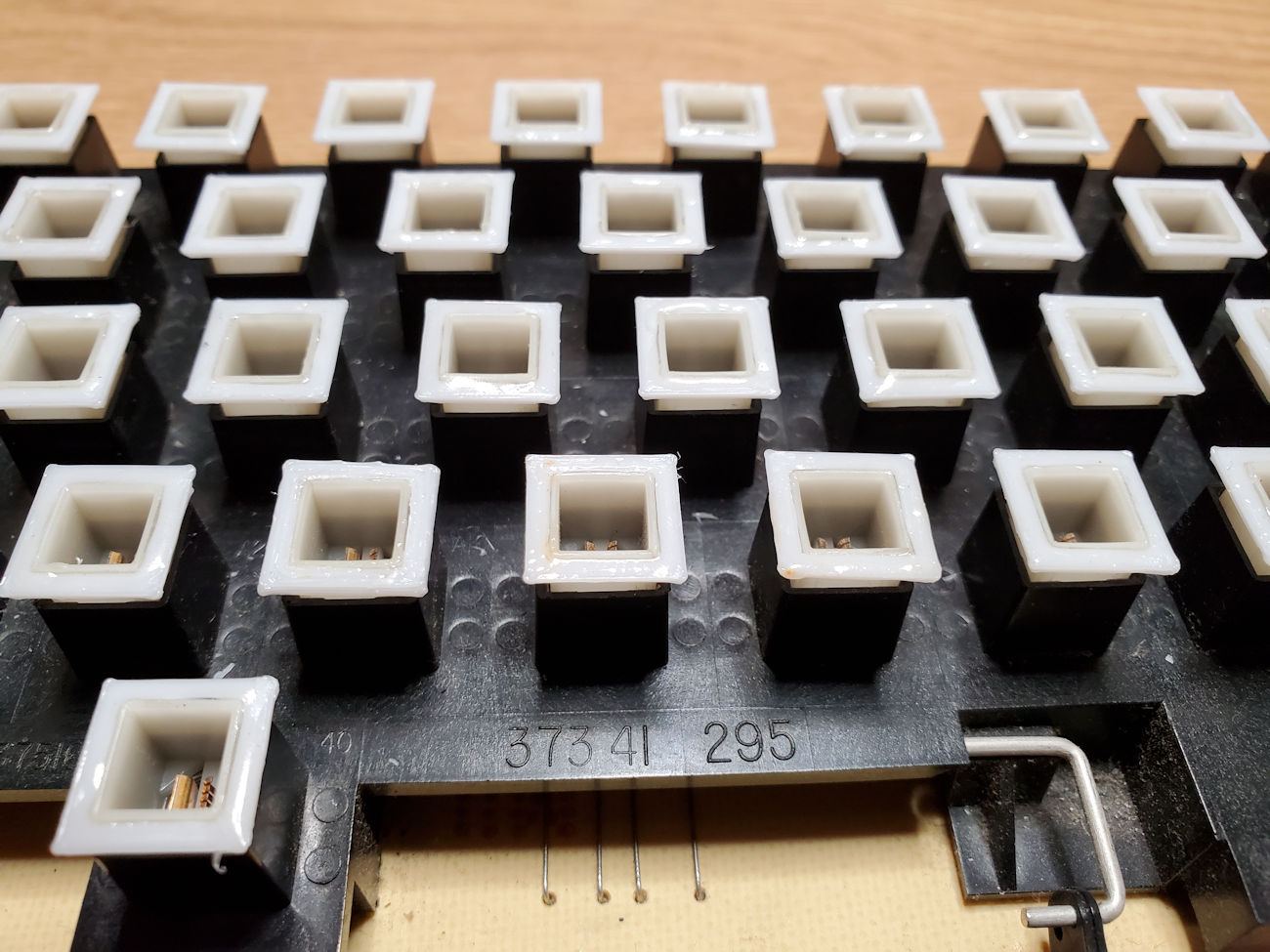
Once you get past looking at the 40 years of dust and debris, you will see that I have removed the W key.  See where the plastic sleeve is split on the top left corner?  That is our problem with most of the keys on the keyboard.  When pressed, the white plastic sleeve binds up on the outer key housing.  The W keycap in this case seats inside the inner white sleeve so it pushes the walls of the inner sleeve outward making it bind up on the housing.  It is this inner sleeve we will repair.  As there is no good method of simply gluing the split sleeve back together, we will put a plastic collar around the inner white sleeve.  The issue we face with this approach is twofold.  First, we must maintain the inner sleeve downward keystroke.  It is this inner sleeve that moves to provide electrical contact of the key.  Second, the keystroke distance itself will be diminished by adding the collar, and it becomes critical to position the collar consistently across all of the keys to maintain a balanced typing experience.

Disassembly

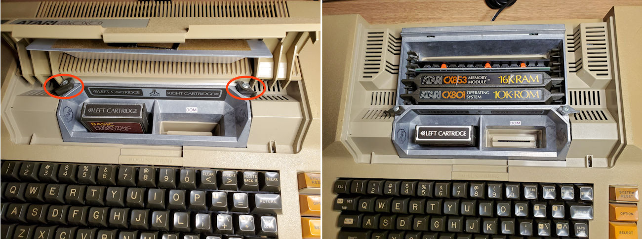
The first step we want to take is to open the cartridge door and unlatch the OS/RAM cover.  Remove this and set aside.  This exposes the OS/RAM cards which we also want to remove and set aside.  While it is not necessary to remove the OS/RAM cards, I do it just to be safe from them falling out and being damaged.

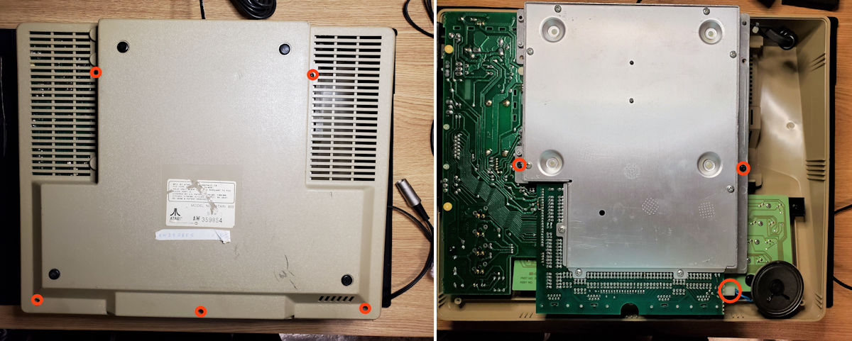
Remove the five screws from the bottom of the case to allow you lift the bottom case up and remove completely. As you will see the computer chassis is still secured to the case top by two additional screws to be removed.

While still having the bottom of the computer chassis exposed, unplug and remove the small speaker and set aside.  At this point, you should remove the two screws noted in the photo and be able to lift the front of the chassis up enough to carefully disconnect the keyboard cable. Once disconnected you can carefully remove the computer chassis assembly.  Note: You will need to remove the cartridge door assembly on the top of the case to be able to effectively lift the chassis assembly from the case top.

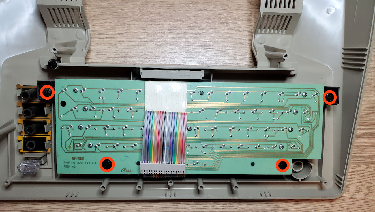
Our next step is to remove the keyboard from the top cover by removing the four screws attaching it in place.  You can set the top cover aside once completed as we are just working on the keyboard itself.

Repair Work

Okay, now it is time to do the repair work that this project is all about, which is to install collars on the white inner key sleeves.  This turned out to be tedious work. The installation of the collar on the key sleeve took upwards of three minutes per key even after practice.  Some took much longer due to the exact tolerance of the collar dimensions.  You don’t want to force fit the collar as it will break, but make a best effort to square up the key sleeve to its original configuration.  This is much easier said than done.

The tools I ended up using for this project were a fine point angled tweezers which I used to provide the precision placement of the collars.  Just needed that small fine point that my fingers just couldn't provide.  A flat tipped tweezers which I used primarily to get a leveled position on the key sleeve once the collar was put in place.  Angled needle nosed pliers as I needed something to grip the key sleeve in some cases with no other way to do it.  And of course, the Bondic UV activated superglue which you can get from Amazon for about $15.

So, let’s get started.

I removed all the keycaps.  Since I have them removed, I might as well wash them up to clean off forty years of debris deposited.  They are just friction seated in the key sleeve.  Also, before going further after test fitting a few collars, I cleaned up keyboard of any debris deposited from the past and gave it an alcohol rub down just to remove any other oil and grease deposits that may have been there.

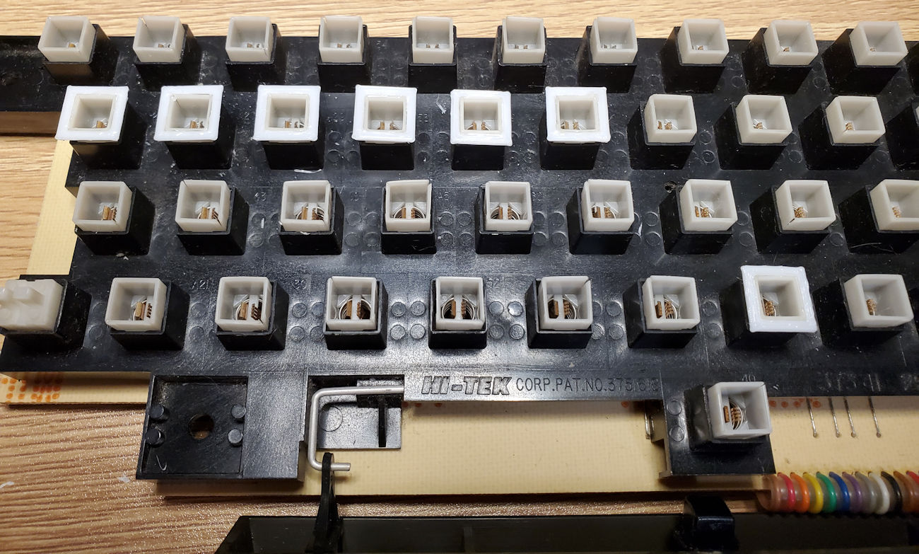
So the next thing to do was attempt to install a few collars and work out my approach.  It was a bit of a challenge to get the collar to slide over the key sleeve as it is a very tight fit.  It is why on a few occasions I needed to use the pliers just to grip the key sleeve enough to get the collar in position.  On other keys sleeves, I pressed into the sleeve with the point of my tweezers and positioned the collar with my fingers.  Once I got the collars in place and positioned to look best, I took the UV superglue and applied it much like you would if caulking a window or bathtub.  The glue remains liquid until you hit it with UV light and then hardens up.  Below is a picture of my first run at this.

The above picture shows just how bad some of the sleeves have split.  Not only does that facilitate keys sticking, but it is this sleeve that holds the keycap in place.  And with this split the keys will pop out with little effort.  The collar when properly placed restores the tight dimension providing the friction needed to keep the keycap seated.


Just to do these seven collar installations in the above picture took over an hour as I worked out how I could best get the collar over the sleeve, leveled and positioned as close as possible to the top of the sleeve so that it provided sufficient keystroke distance to make the electrical contact when the key is pressed.  Things moved a bit faster once I got the process I used worked out.

I worked on this over the course of three evenings and it ended up being about 4 hours work to complete the collar installation.

You can see in the above picture where the UV superglue is set.  While the UV light will set this glue effectively in about 12-15 seconds per key, I generally walked the light around the key for about 30 seconds to ensure all the glue is activated.

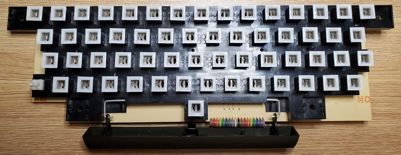
All key sleeves have been collared and I tested without the keycaps installed to validate connectivity before finishing up with putting the keycaps back in place.

All keycaps installed and checked for proper function.  No sticking keys!!  And that was the goal of this project.  Now to put everything back together and complete this project.  Reassembly is the reverse of disassembly so I will not go into those steps here.

My Takeaways For This Project

  • Plan on this type of project to take some time and don’t let it frustrate you. Getting the collar over the key sleeve is the most challenging.  And once you get the collar over the key sleeve, plan time to position the collar to the optimum topmost point in the sleeve without it popping off.  Yes, that happened regularly to me and I had to start the whole process over again.
  • Taking from my first takeaway, it is critical that you position the collar as close as possible to the top of the sleeve while still providing a surface for the UV glue to adhere to when activated. If you position the collar too far down on the sleeve, you not only will have an inconsistent keystroke across the keys but may prevent the key from making the electrical contact needed to make it work.
  • Working with the Bondic UV superglue worked well overall but as I used this glue, the tube started leaking from the tip when not needed. Gets a little messy as it has the consistency of honey.  Since it does not harden unless you hit with UV light, will continue to be a bit sticky while in use.
  • You do lose ever so little of the downstroke of key when the collar is in place. I doubt someone who had never used this keyboard would notice it, but as I like a long downstroke on my keyboard, it does stand out.  Still, it works fine and does not impede its use, its just my preference.

Upgrading My Atari 800XL With Ultimate 1MB and UAV

I decided to upgrade one of my Atari 800XL computers with an Ultimate 1MB FJC firmware board and a UAV. I will be using a stock fully socketed Chelco branded mainboard 800XL computer for this upgrade.

The Chelco mainboard pictured below is out of an 800XL that would not allow myself to drop out of BASIC. It had also exhibited other strange issues such as bad memory, but never in the same location during tests. As I was unable to find the problem(s) with this board, I took it to my T.A.C.O. meet up some time back to have John Hardie take a look. John subsequently could not track down the issue either, and gave it to Raymond Jett of Classic Arcade Components to see if he could find the problem. After a few hours and not getting the desired results, they were about to give up when Raymond happens to look carefully at the PBI circuit traces and found ever so slightly shorted traces across the PBI. You can see where Raymond cleaned up the circuit shorts and then used a bit of green nail polish to cover and protect the circuit trace. This solved the board issues.
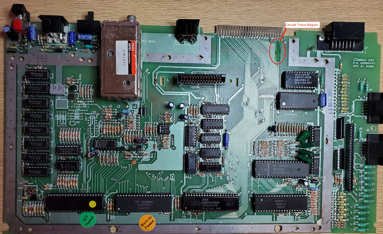
My Chelco branded 800XL mainboard prior to any modifications being made.
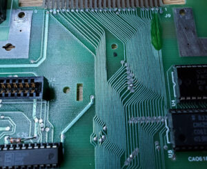
A closer view of the circuit trace repair on the mainboard
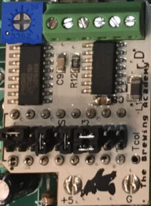
Ultimate Atari Video (UAV)

My first objective with this project is to install the UAV (Ultimate Atari Video) from the Brewing Academy. The UAV greatly enhances the video output of the Atari with a more refined composite signal and adding S-Video. For whatever reason, Atari neglected to add the Chroma signal to the output DIN, and only supplied Luma and Composite.

UAV (Ultimate Atari Video) Installation

For the UAV I won’t go into much detail of the installation procedure as that is very well documented in the provided instructions both in paper and digital form. I am basically lifting a couple of chokes and replacing the 4050 CMOS chip with the UAV circuit. This is my third UAV installation as I have already installed the UAV in a different 800XL and a 600XL. The 600XL in its original state does not include a monitor (DIN) connection or circuit components, just RF for connecting to a TV. It does have the component silkscreen and circuit traces prepped, just no components installed. I will write up on that machine later.

The first step of the UAV installation is to identify the connection points and prepare them accordingly. You will see in the following photo the CD4050 chip we will remove, and this is where the UAV board will plug in. Also, the two chokes will need one side lifted from the board as we will use those pads to connect a couple of wires going to the UAV. And finally, the connection for the Video In on the board as well as the ground location we will use.
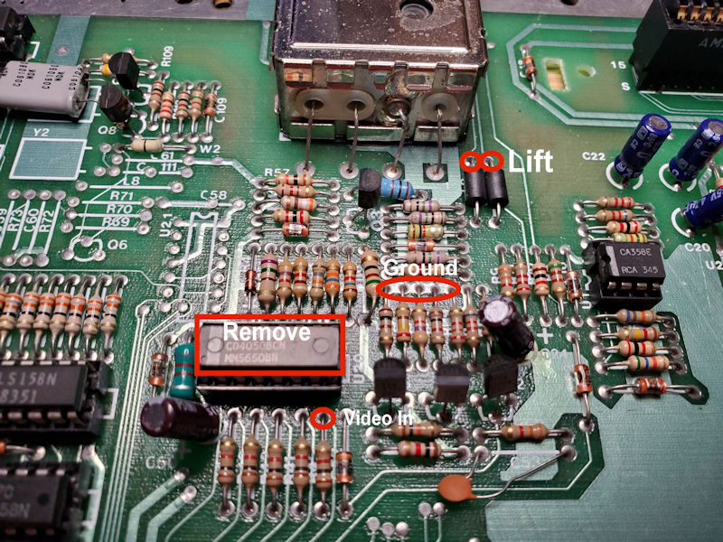
UAV connections I will use for this project.
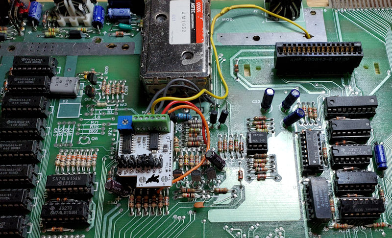
UAV installed, notice the yellow wire?  It goes thru an open hole on the board.

This is the UAV installed, and the yellow wire is the Chroma signal. The first installation of a UAV I did, had me connect the Chroma wire to pin 5 of the DIN connector on the top of the board. I found it to be a rather sloppy connection as the wire and solder used just would not adhere to the pin very well. Maybe I should have used more flux, but it just looked like a big glob of solder sitting there. On subsequent installations such as this one, I ran the chroma signal wire to the bottom of the PCB pin 5 solder pad and while the wire may be longer, it was a much cleaner and secure connection.
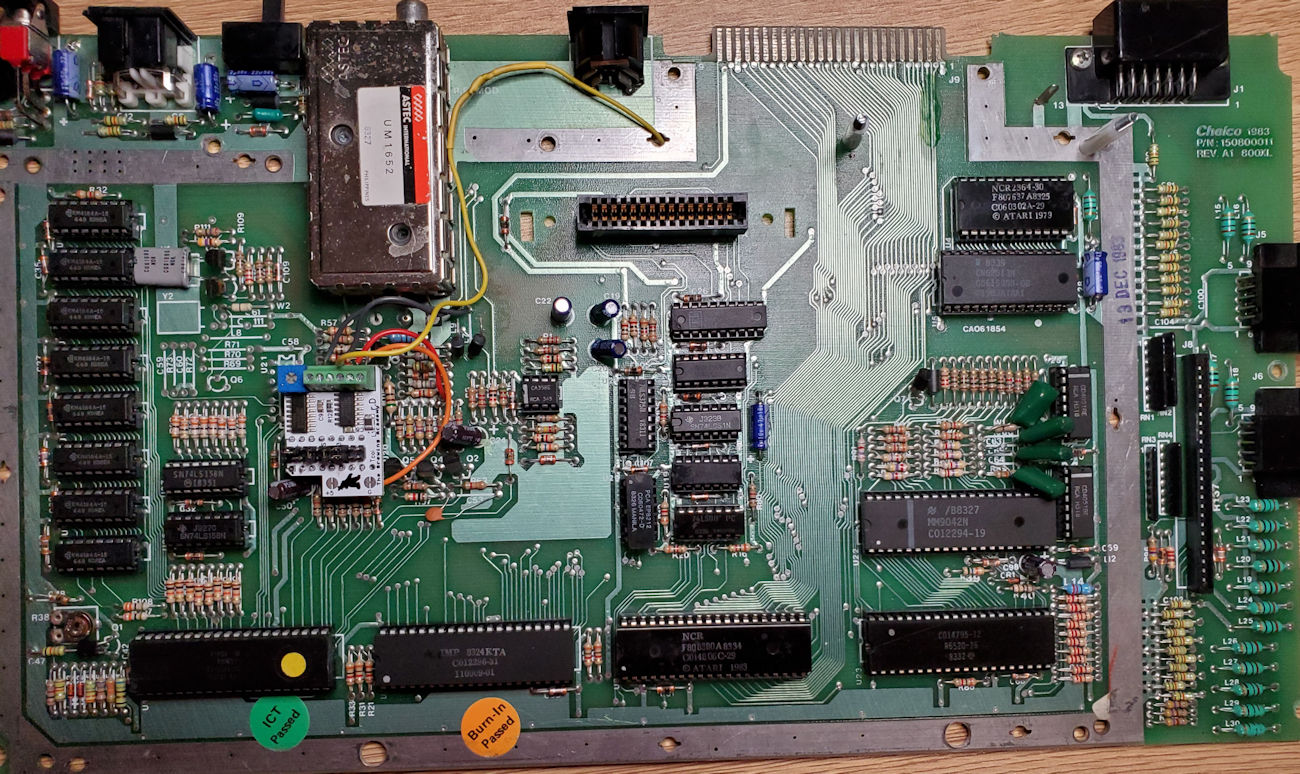
Full board view with the UAV installation completed.

Installing the Ultimate 1MB Memory Upgrade
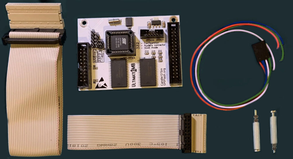
The typical Ultimate 1MB Installation Kit

This is the Ultimate 1MB FJC (Flashjazzcat) firmware kit much like I received from Lotharek. As the picture shows, you have the Memory/OS board, a 28-pin ribbon cable for the OS socket, a 20-pin ribbon cable for the MMU socket, a 4-wire cable for connecting to the various CPU points, and 2 standoffs for mounting the memory board in the computer.

So, what is the Ultimate 1MB upgrade? As the name implies, this board expands the stock 64K RAM (required) computer up to 1MB RAM in a few different memory configurations, 1088K RAMBO, 576K CompyShop, 320K RAMBO, and stock 64K. This greatly extends the capability of the XL/XE computer that allows for running any programs requiring more than 64K memory such as AtariWriter Plus XE which requires 128K minimum. This board replaces the stock operating system (OS) ROM with a few different OS options including, XL OS 1.3, XEGS OS, Altirra OS 3.20, and Atari OS B PAL. The U1MB provides a real-time clock with the date and time compatible with the R-Time 8 cartridge format from years ago. SpartaDos X is built-in with a boot option that takes advantage of the real-time clock feature. And for my 800XL computer replaces the BASIC (rev. B) with the following programming language options that include, Atari BASIC (rev. C), Altirra BASIC, Synassembler, and Atari Assembler Editor. All of these options can be configured at boot and saved as one of four available profile defaults from a nice menu interface when you hold down the Help key upon power up. There are more advanced options for the BIOS, and this board also takes advantage of the SIDE3 cartridge, plus some PBI functions for which I have not explored.

The first step to mention is planning where you want to put this additional board in the computer. On the Atari 800XL the most common installation point is seated over top of the OS and BASIC ROM sockets. Depending on how many different modifications you do to your 800XL, it may require a different location. I will do as is the common practice of the Ultimate 1MB location.
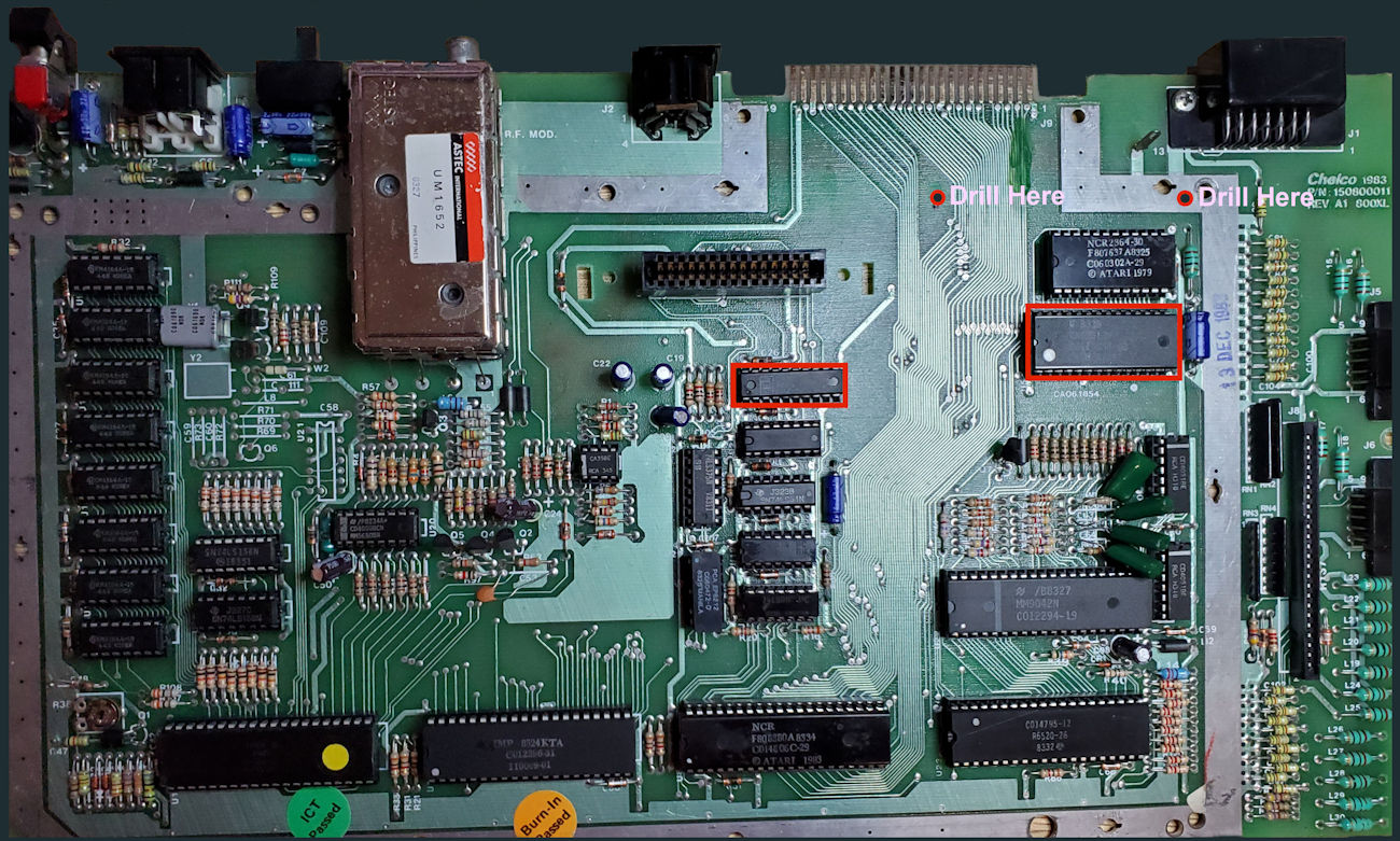
Note the locations for the U1MB board mounts, MMU and OS ROM.

Above you see the two points for which we will drill holes for the standoffs and the MMU and OS chips we will remove.

Step 1. Before I began the electronics work, I drilled the two holes that I will use for mounting the U1MB to the mainboard and did a test fit. Do be careful with drilling the holes so as to not drill through any circuit traces. Check both sides of the mainboard if you attempt to install it in a different location.
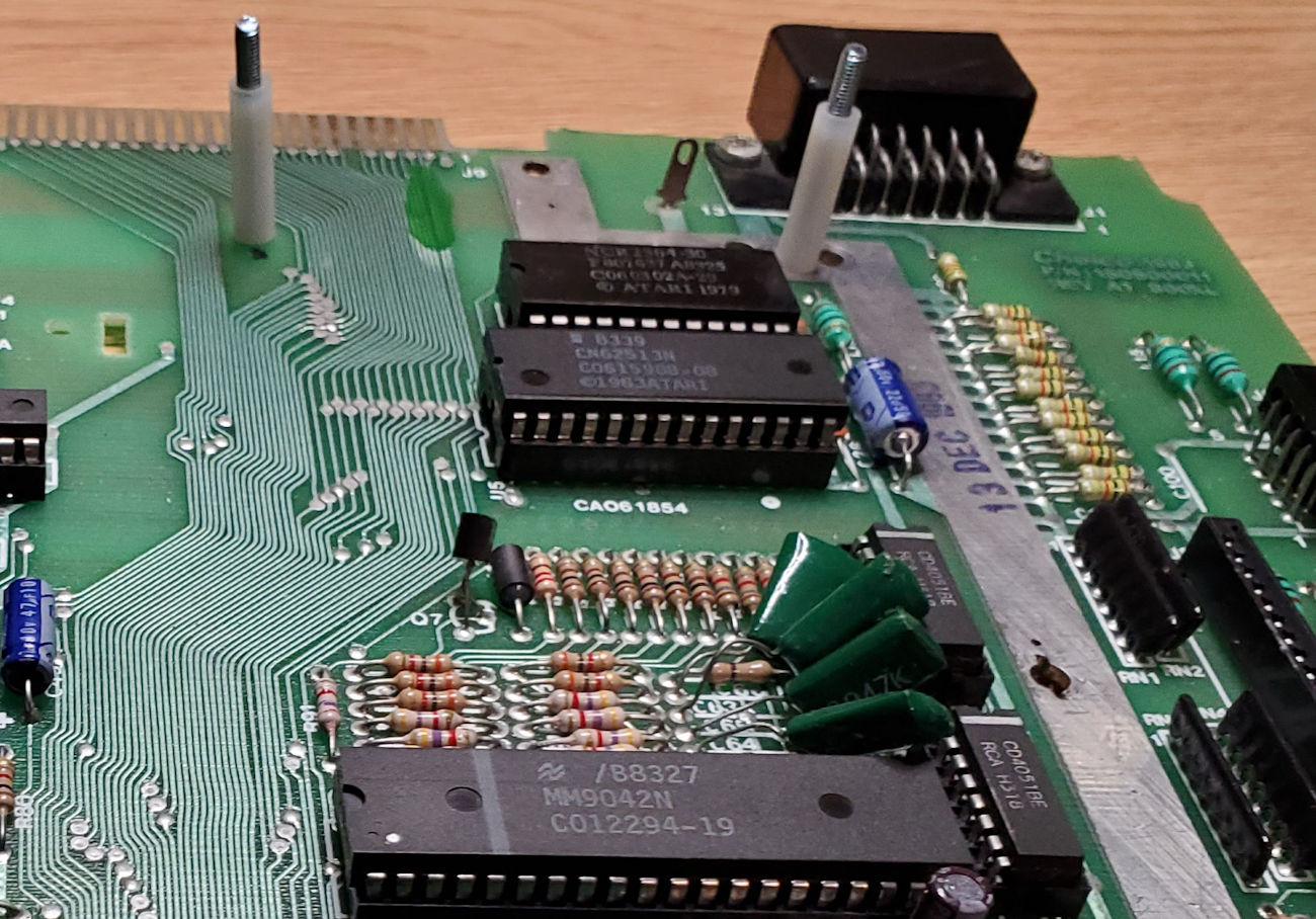
Board Mount Standoffs inserted for a test fit.
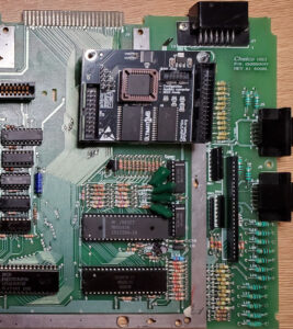
Loose fit of the Ultimate board.

After I drilled the holes, I inserted the standoffs and then put the U1MB on the standoffs just for a test fit to make sure I had the alignment correct. Note that the U1MB will extend over the existing BASIC ROM and OS ROM. There is no need to remove the BASIC ROM for this upgrade in the 800XL and it can remain in place. What is particularly nice about this upgrade is you can easily revert to your stock XL computer configuration by simply unplugging the U1MB and installing your old MMU and OS chips back in the sockets.

A bonus for this project is that the 800XL motherboard I’m using is fully socketed. This means that I I don’t need to desolder the MMU or OS chips from the board and install sockets for use of the U1MB. If your board is not socketed, it will be a bit more work, but well worth it. But for myself, it means in my next step I only have four wires to solder in place.

Thus far, of all the upgrades I have made to my Atari computers, this one is by far the simplest to do. As an example, my Wizztronics 256K RAM upgrade for one of my other XL computers required removing a resister (R32) and lifting 5 pins of the PIA chip (12 thru 16), soldering wires to each of the 5 pins that go back to the RAM upgrade board which replaces the LS158 chip. Removing all of the 4164 DRAM chips and replacing them with 41256 DRAM chips. This is where you hope your board is socketed or you will have a lot of desoldering to do. To top it off, if you want to revert to your stock XL computer it becomes a much more complex project. I state this for clarity of how much simpler the U1MB is to install even if you must desolder the MMU and OS chips. And to revert back to a stock machine is no more than unplugging the OS and MMU cables to put the old chips back in place.

Step 2. Soldering the four wires that will plug in to the U1MB is made easy as others who have installed it previously show you the solder pads to use. In the first diagram I have adjusted the wire color I’m using that will correspond to the header on the U1MB. The next diagram shows the standard 800XL mainboard again where my wire colors match up to the solder points on the board. As wire colors may change via the vendor batch shipped, it might not be the same from one installation to another. Just match your wire colors accordingly and you’ll be fine.
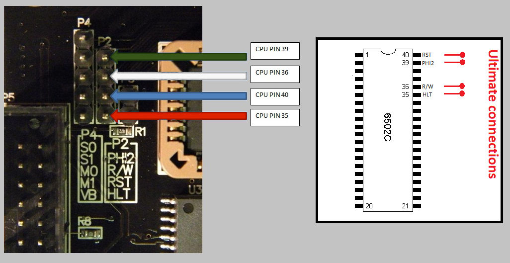
Ultimate CPU header connection diagram.
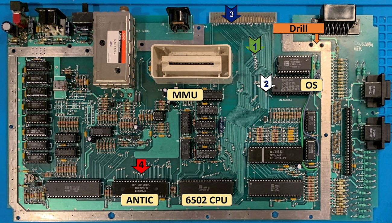
The points show where I will solder the four wires on the board.

The connection points above are not the only location that can be used, but for my installation were the most convenient.
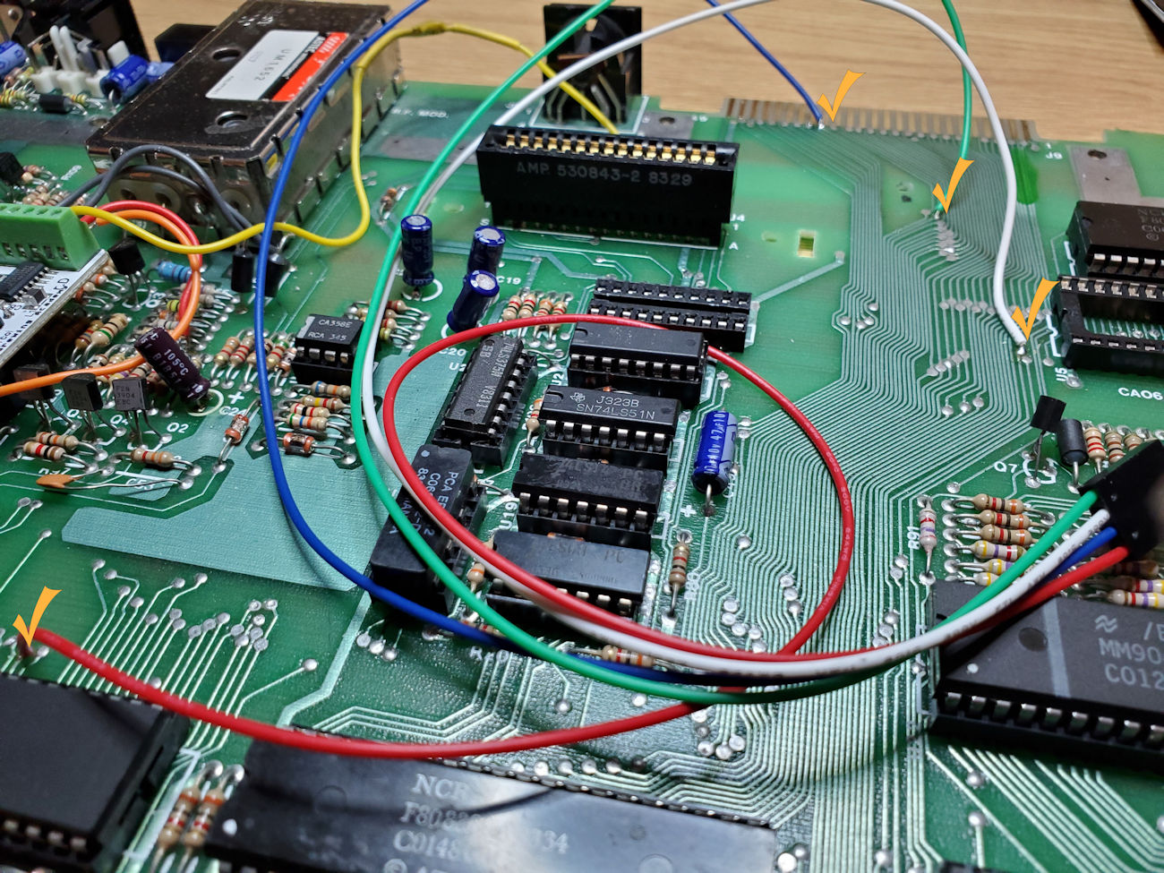
My solder work is completed!

That is all the soldering I had to do. Just those four wires as shown above. If you look at the picture, you can see I have already removed the MMU and OS chips. All that is left to do now is install the cables and board to finish this project up.

Step 3. This could be said to be the most difficult step of the project. Now I need to plug everything up which itself is not an issue. However, the cabling that comes with the U1MB is configured so that you have different options for mounting the board in the various 8-bit machines. For example, in an XE computer the typical mounting point is in the back left side of the computer by the power switch and requires a longer cable run to the MMU and OS chips. So, the installation kit is sort of a one size fits all idea in terms of the cabling provided. I could cut the ribbon cable to a shorter length for a cleaner installation, but I lack the ribbon cable connectors in my stash of parts. So, if I don’t properly disassemble the connectors (break it), I’m going to have to order replacement connectors. Or if I cut the ribbon cable too short so I can no longer reach my connection sockets, I must order more ribbon cable, and probably the connectors to go along with that. Just a bit too much of a hassle for my first-time installation. Maybe in the future I will look to clean up the cabling so that it looks factory fresh. 😊

Okay, first I lay out the cabling in a manner that lets me plug in to the sockets and route to the U1MB board. Then I plug the ribbon cables into the MMU and OS socket first as the U1MB will sit over top of the OS socket making it a bit of a challenge to plug in after I were to mount the board. Next, I loose fit the U1MB board on the standoffs and route the OS ribbon cable from underneath the board to the top connector paying attention to where pin 1 goes. Then the ribbon cable from the MMU needs to plug in to the U1MB board again paying attention to where pin 1 goes. The final part is to plug in the 4-wire header connector being mindful of color code chart I used previously for soldering to the mainboard. Really don’t want to plug any of this in backwards.
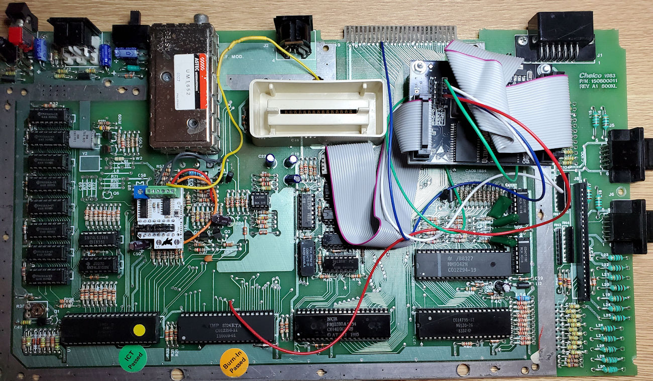
Everything installed for testing.

Before I go further, its time to test my work prior to putting the board back into the computer case. So, the above is just a loose fit of the board and cables just to make sure it works.

Well, here it goes as I flip the power switch…
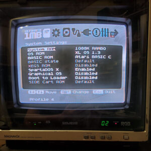
Successful Boot! Everything is wired correctly.

Success!!

Isn’t it interesting how my phone camera picks up all the Moire from the CRT screen. In person it looks a whole lot better than what you see here. The image is clear and sharp. I will have to take a picture when I connect to an LCD/LED display. Wonder how it will look on my 65-inch 4K QLED in the living room? Not that my wife will let me use it there and get in the way of her shows or anything like that?

This would be the default configuration of the U1MB which can be configured with the different OS options and ROMs as noted previously in this project documentation.

Since the loose testing was successful, it is now time to tighten things up and tidy it up as best as possible.
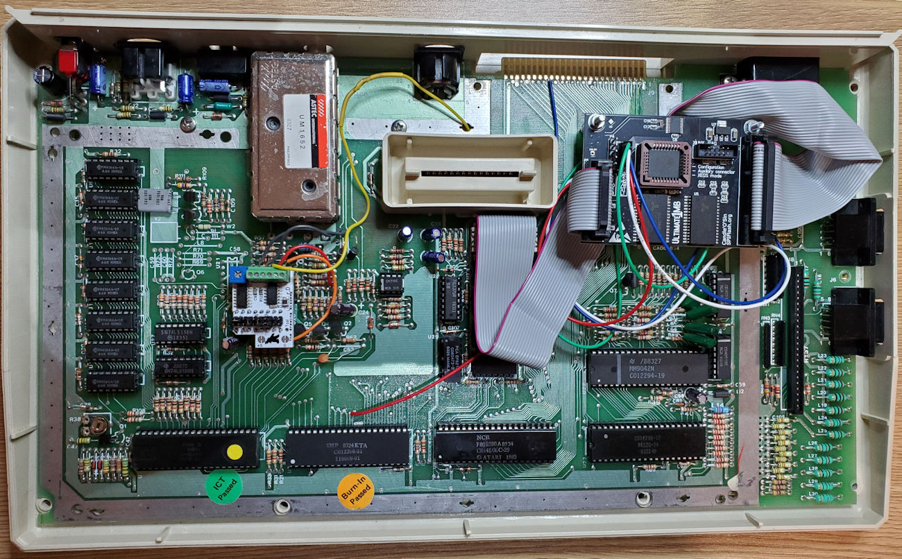
Mainboard is back in its case bottom. Time to close it up.
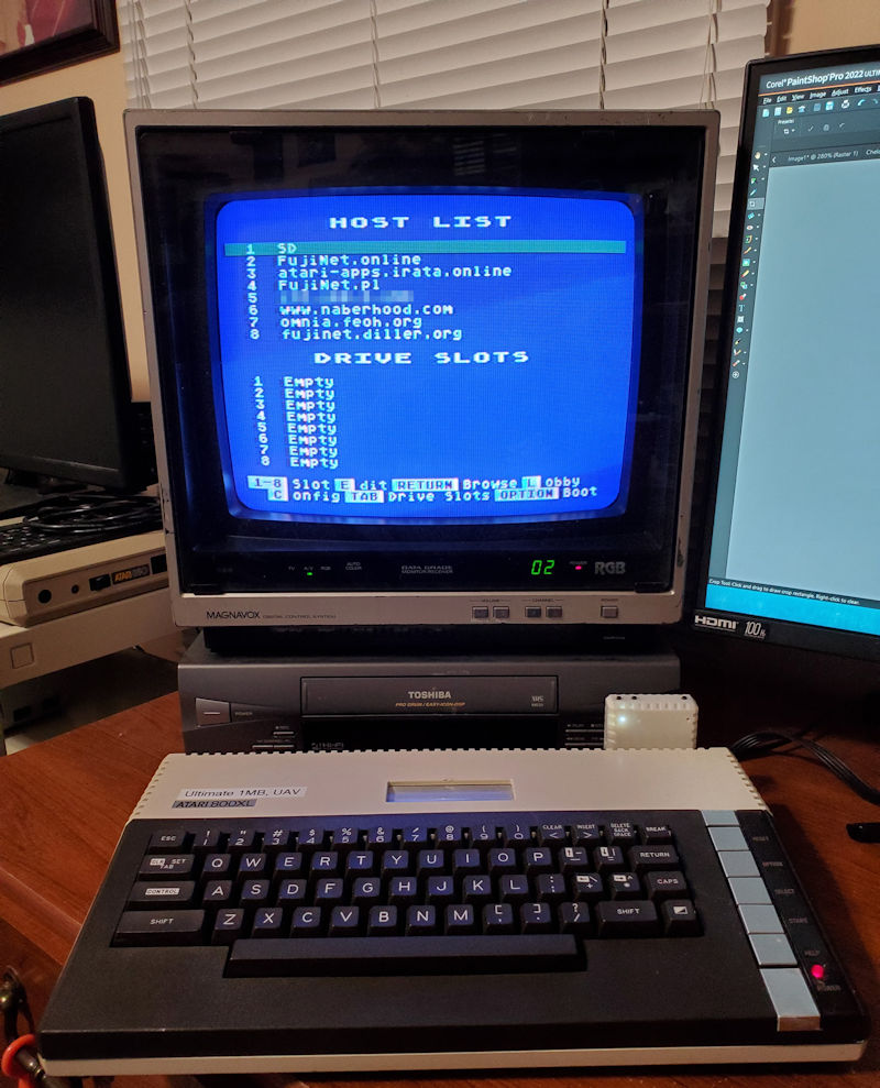
The finished product up and running.

And here is the completed project up and running. To recap, we have an Atari 800XL that was modified with an Ultimate Atari Video (UAV) to provide for sharper composite, and S-Video by providing both Chroma and Luma on separate signal paths.

Next is the Ultimate 1MB (U1MB) with the FJC firmware. This not only adds more memory to the computer allowing it to run any Atari 8-bit program requiring more than 64K of memory, but also adds options for different versions of BASIC, and Assembler languages. And that’s not all, you also get a real-time clock as well as Sparta Dos X built in. These two items work hand in hand allowing you to use date and time stamps on files and work well with programs looking for a clock/calendar function. The U1MB is geared for use with what is called a SIDE3 (SIDE2 is an earlier version) cartridge, which in its most basic form is a hard drive on a cartridge. It too does many different functions and is popular in Europe which is where the U1MB was designed and built.

Finally, we have a Fujinet connected to the SIO port of the computer. You could call this the New Kid on The Block of end all be all devices. The Fujinet provides wireless connectivity to the internet, mass storage for all your Atari programs and data. Incredible printer emulations that mimic a host of printers from back in the day to perfection. And as it continues to be developed, you can interact with other 8-bits such as the Apple II, Coleco Adam, and even the Commodore. Want to know where the ISS is at right now? Fujinet can show you. Would you like to display the current weather and forecast on your Atari. Yes, it can do that too.

Okay so now I will provide the cost for my project should it inspire someone else to jump on the Atari 8-bit bandwagon.

  • 1 Atari 800XL (I have four so its not a fair question) that if you don’t have can be purchased via eBay from as little as $75 to more than $300. I can only say those asking big bucks, need to show me some fantastic reason why I would pay that much. But lets just assume $150 as a nominal cost.
  • A Fujinet can be purchased from The Brewing Academy for $80 which includes shipping and a tip. Works in any stock Atari computer that has at least 32K of memory. Atari 400 and 600XL computers came stock with 16K and would need to be upgraded to use this.
  • An Ultimate Atari Video (UAV) which is clearly optional, can be purchased from The Brewing Academy for $40 delivered. Just provides sharper video especially if you are hooking up to modern TV’s or monitors.
  • The Ultimate 1MB with the FJC firmware purchased from Lotharek’s Lair in Poland for $130 that includes shipping via Polish Post Express. This amount may change a bit depending on the conversion rates of polish PLN at the time of order. I received my U1MB in just 15 days from order which is not bad.

So total to expect to pay should you need to buy an Atari 8-bit computer: $400.00

Some takeaways from this project for me.

  1. Since this is a hobby of which I collect Atari computers, I don’t mind modifying a unit if I have one that remains standard built. I have one 800XL which will remain stock and I keep as a show piece.
  2. As I do more of these modifications and repairs, my soldering skills are improving and am learning different methods to repair or maintain my 40-year-old equipment.
  3. This project was a great deal of fun as I just took my time with each step. So much so that I’m now breaking my own rule of maintaining one stock computer for each model as I’m upgrading my only 1200XL with all the above. Guess I need to go find another 1200XL out in the wild to put my first rule back in order.

A.P.E. Atari Peripheral Emulator

In the mid-90’s, I was still actively using my Atari computer(s) mostly for playing video games at the time.  I was using it in the original manner with the disk drives and cartridges I owned.  But technology had evolved and the internet was just beginning to take off and I like many others were looking for ways to modernize how we used our beloved 8bit computers.  Some time during my search I came across instructions on how to make an SIO to PC RS232 cable that with software some smart individual(s) had developed to allow you to save and load all your programs that were traditionally on a floppy disk to and from a PC.

At this time I attempted and was marginally successful at building the SIO2PC cable and using the software I had originally found available.  However, it was still not quite ready for primetime use and standards of file formats did not always match up to what I was looking for.  Then I found information about some guy named Steven Tucker and his program A.P.E. (Atari Peripheral Emulator) and wow!  I was impressed.  His program and the corresponding SIO2PC (Ape Interface Cable) was just what I was looking for.  DOS based at the time and his cable instructions were slightly modified from what I had first attempted to use.  It was with this program and the cabling information he provided that allowed me to archive almost all of my Atari disks to a PC file that I could then load/save on my Atari computer.
In 2003/04 I retired my Atari collection and put all in storage not to be touched again until the Pandemic of 2020.  Locked down with extra time on my hands, I started pulling out my old computers and once again began to revive the enjoyment of my past.  With that came the search for an update to what A.P.E. was in the day and I quickly found that Steven Tucker was still improving his product and A.P.E. was now Windows based and he had further developed a USB SIO2PC adapter.  Cool!  Ordered up and began to once again enjoy those times of my past.  So much simpler then.

Site Setup in progress

Just now setting up this site for use.  Blogging is not something I have done much of before so it time to learn and get comfortable with the process.  Just going to make adjustments with the site as I go.