
Atari Cheep Talk – Analog Magazine, Issue 29, April 1985
In the Analog magazine April 1985 issue there is an article on page 59 titled "Cheep Talk: Build your own speech synthesizer” by Lee Brilliant. Back then, I did not have the money or patience to build this “Cheep Talk” device but was fascinated by the article. So, I Xeroxed the article and stored it in one of my paper binders. I must have borrowed the magazine from someone else as I never had a subscription to Analog, or recall purchasing this issue.
Recently, I was perusing through one of my binders and ran across the article. Today you can read all the Analog magazines as they are freely available on Atarimania, or the Internet Archives, amongst other places. As such, I jumped on over to Atarimania and looked up the issue in question and decided to attempt to build this Cheep Talk device that eluded me back in 1985. What follows is my attempt at constructing this device just as described in the article.
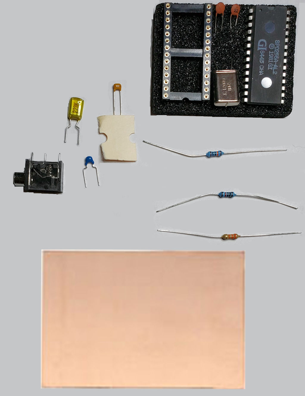
My first objective is to acquire the parts needed to construct this device. The main component that is needed is no longer manufactured as it is a Radio Shack (General Instruments) SP0256-AL2 speech chip. You can still find these on eBay as New Old Stock (NOS) and I picked one up for $57 which also includes two 22pf capacitors, one precision IC socket (nice touch), and one 3.12MHz crystal which is the original crystal planned for use by the author at that time but was substituted by his parts list. All the other components are readily available from places such as DigiKey, or Jameco. And since I stated I was constructing this project just as was from the magazine article, needed to get a single sided copper clad breadboard that I will use to make the circuit board.
Cheep Talk Components
I will provide the full list of the components needed/used at the end of this post, but to summarize, it is 3 resistors, 5 capacitors, 1 crystal, the SP0256-AL2 Speech Synthesizer IC, and the PCB. To make this functional beyond the electrical components will also need 2 DB9 serial connectors and an amplified speaker of some sort.
Circuit Board Construction
It has been 25+ years since I did anything with PCB etching and technology has really changed for the design process. The home DIY boards made from back in the 80’s from when I learned to do this would make use of etchant resist pens (Sharpie’s) and rub on transfer tape that would cover the copper with your circuit design. Today the expectation is that you build your circuit in one of the many CAD programs available and then transfer that circuit to the PCB via printout using a hot or cold printer toner method, or by use of photo developed PCB method. Rub-on circuit transfer tape is no longer manufactured and of course you can still use the Sharpie method, but still must deal with the flaws of this approach.
For my first attempt I opted for the Hot transfer toner method. Since the circuit design is provided in the magazine article, I only need to print it out in mirrored format on glossy magazine paper (cheap way to do it), or on vinyl print paper which allows for better visual of the circuit printed as you don’t need to read thru the already printed text/graphics of magazine paper. As my vinyl print paper had yet to arrive, I decided to give this magazine paper a try.
As mentioned above I’m doing the Hot transfer method (toner) which requires that we first print the circuit to be transferred to the PCB via a laser printer. Inkjets will not work for this approach as it is the toner of the laser printer that will be deposited to the copper of the PCB from the paper. Keep in mind that you need to scale the printout to match the actual size of the circuit traces intended. This is critically important for IC socket connections as pin location needs to be accurate.
An issue brought up for the above method(s) is that the Brother Laser printer(s) of which I own do not do a good job of toner distribution for this application. I can confirm that in my case this is true. I don’t think it is the toner distribution as much as it is how the Brother technology deposits toner on print medium. So, it may not really matter if you are using OEM Brother toner cartridges, or a generic brand. In any case, the printout was not of high quality.
The next step in this process is to take your circuit printout and position it print side down on the copper PCB of which you will want to etch the circuit. Next you get your trusty clothes iron, you know the one that has been sitting in the closet (or in my case the garage) the last 10 years collecting dust and put the heat setting to around 170 degrees. I got my digital thermometer out just to be as accurate as possible. You then start ironing on the PCB for 5 to 7 minutes. It is a good idea to put a cloth of some sort over the print medium you are using as we really are not looking to start a fire. We just want to use heat and pressure to deposit the toner from the paper on the copper of the PCB. Once done, let the PCB cool off for a few minutes.
Now we carefully peel back and remove the print medium from the PCB and if all went well the toner has adhered to the copper of the PCB forming your circuit trace. In my first try it looked to have done a fair job, but I did have to go over most of the traces with a Sharpie as there was copper still visible in many locations of the circuit trace. I let the Sharpie ink dry for about an hour and then attempted my first etching. I’m still using the tried-and-true Ferric Chloride solution and about 15 minutes later had to take the PCB out of the solution and rinse off.
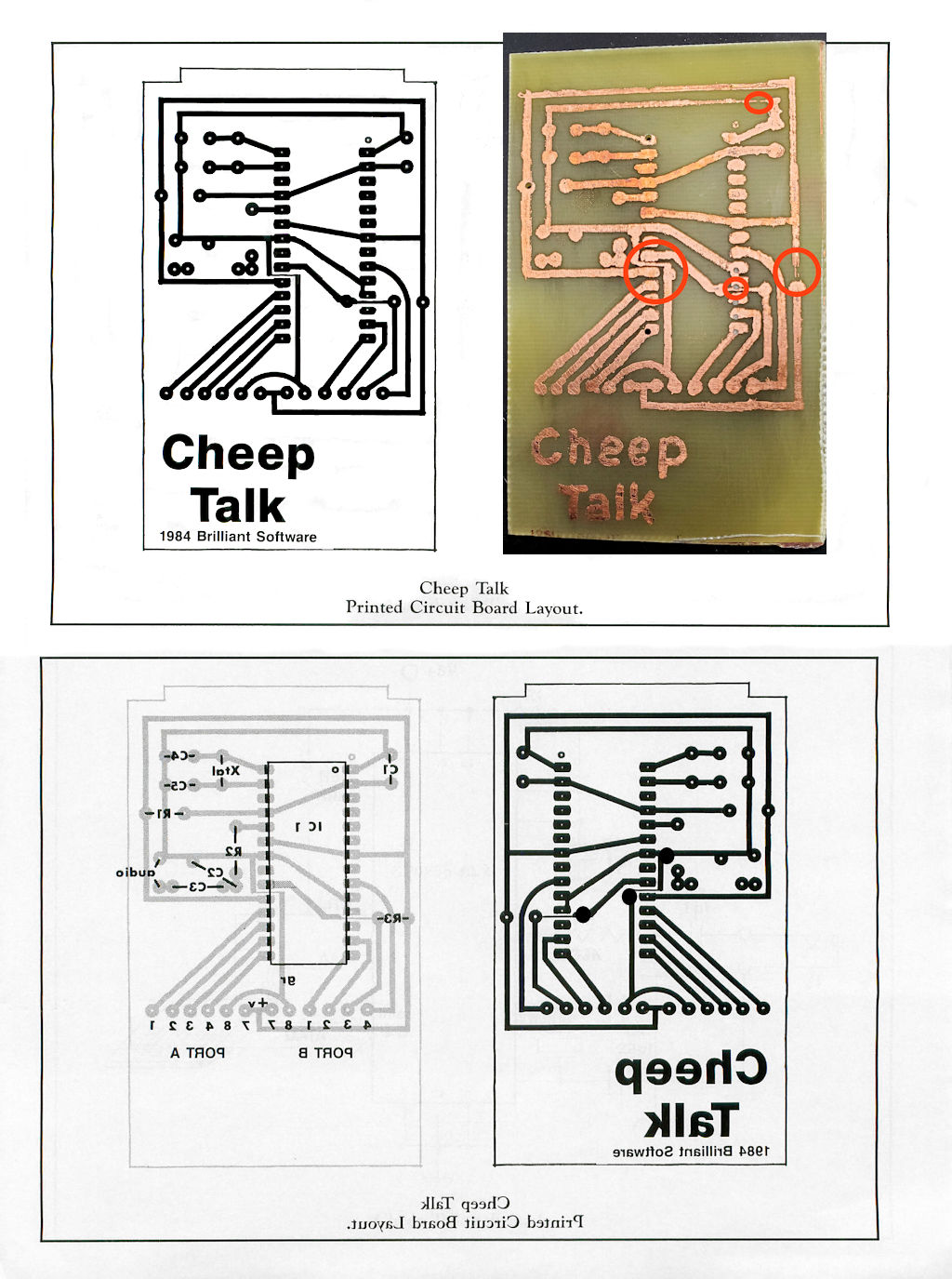
The above picture shows the circuit diagram from the magazine article and my first run of the PCB etch. I circled all the issues in RED for the PCB.
- The most challenging issue is with etching away too much of the copper as you can see the circuit trace has a gap. This was always a concern when you did not have enough coverage with the etch resist pen and/or transfer tape years ago. It makes timing crucial of the etching process to remove all the exposed copper, but not what you traced on the board.
- The next issue of which I noticed and attempted to plan for is two circuit traces going in between the IC socket solder pads. For the home DIY’r that’s a really fine line needing to be etched. I had planned for this and added solder pads to the circuit with the expectation that I would use jumper wire to address this challenge. Also, these circuit traces are so close to the IC socket solder pads, chances are very high I would have solder jumping over on to the circuit trace and shorting it out.
- And of course, with the DIY approach of using etch resist pens and my Brother laser printer, my circuit traces are far from precision. But this first attempt let me work out how to drill the holes in this board. You can see where I misaligned an IC socket template I used on this board and ended up drilling off center and through circuit traces.
My second attempt at etching this board went better. I used the same Hot Transfer method as my first attempt but with vinyl print paper as the medium to deposit the toner. It is clear that the Brother laser printer is not very useful for toner transfer PCB projects. I did have to do a lot of touch up work to the board with a Sharpie prior to etching.
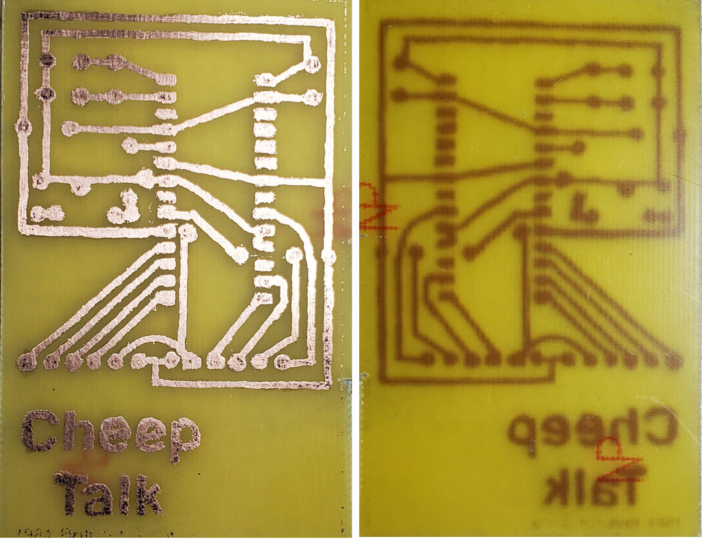
I did find that removing excess toner from the board takes more work than the Sharpie solution. Steel wool or 3M green scrubbing pads are needed. Not a big deal, just more effort than acetone cleanup. I was satisfied with this attempt and used an X-acto knife to address any residual copper tracings left on the board. Next step is to drill the holes in this.
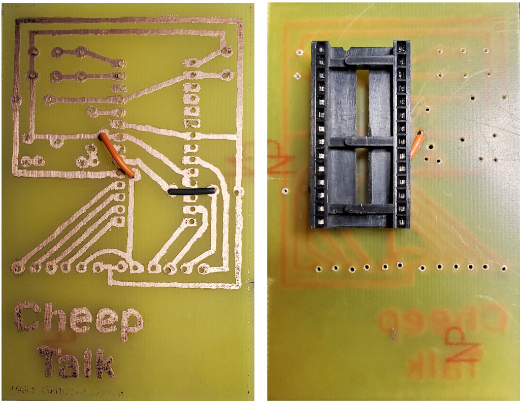
For this board I removed the circuit traces between the IC socket connections in favor of using a jumper wire to complete those two circuit traces. The above photo shows them on the bottom of the board for placement, but I will be installing them on the top of the board. I also decided to use an IC socket with long legs as it provides me clearance to connect the jumper wires on the top of the board and makes it a bit easier to insert the socket in the board as my drilling of holes is not as perfectly aligned as a commercial machine drilled holes.
Installing the Components
My first step was to test fit the components and right off I found that I had forgot to provide a solder pad for one of the jumper wires which was meant to be used for a resistor. In this case I will drill another small hole right next to the solder pad where I can route the resistor wire through to tie into the solder pad. A little more solder to flow over and connect the pad will work if not the prettiest solder joint.
With that SNAFU fixed up the rest of the component placement went as planned. Now on to soldering in place.
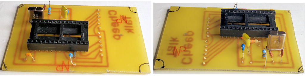
If you look closely you can see where I installed the gray and orange jumper wire on the board through the IC socket pins. The black markings on the edge of the PCB are where I need to cut away to allow for proper fit inside the project case I have. The open holes on the board will be for the two joystick cables and speaker jack.
In the article the author notes that he used an external amplified speaker for the project and cautioned that hooking up to a stereo amplifier could damage the Cheep Talk or your Atari if the amplifier generates additional voltage on inputs you may decide to use. As such he recommends using one of Radio Shack’s small, amplified speaker units. My initial plan was to use one of the many small computer speaker sets in my inventory from years in the PC industry. But then noticed the author also stating that you could use the cassette audio output/input pin 11 on the SIO jack of the Atari and let it play through your TV speakers. And the article further notes that in doing so you only need to use one wire for this as the Cheep Talk circuit is already grounded through the Joystick port cabling eliminating the need for an external ground source of an amplified speaker unit. Upon reading this tidbit of information, I elected to take this approach as I am already hooking up to a TV and will have an open SIO port that I can connect to pin 11 of. Besides, I have many Dupont wires laying about that will fit nicely into both devices.
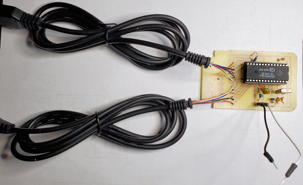
Another change I made was to use standard 9 pin molded Joystick cables as opposed to ribbon cable the author used. Looks much more professional in my opinion.
Putting Cheep Talk In The Project Enclosure
Now that I have finished all the solder work and cleaned up the board, it is time to put it in the project box after doing a little construction work to said enclosure. I needed to cut openings for the cable strain relief plugs and holes for the speaker connection(s). At this point I’m going to leave both connection wires in place should I decide at a future date to connect an external speaker of some sort. It does have to be an amplified (powered) speaker as the Cheep Talk device provides no speaker amplification. This is where the benefit of using pin 11 on the Atari SIO jack makes sense as your TV already has amplified speakers that the audio generated by Cheep Talk flows.
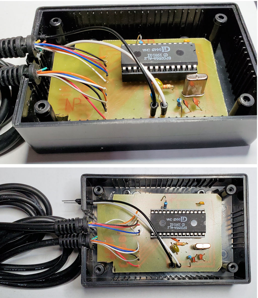
The PCB will be secured to the case with two small panhead screws of which the lip of the screwhead will hold it tight to the enclosure bottom. This way I don’t need to do any more drill holes in the board. Also, the black wire extending out to external connection point is what I use for the audio output to the TV. The white wire is technically a grounding circuit and would be used with an external amplified speaker solution along with the black wire should I ever decide to use it.
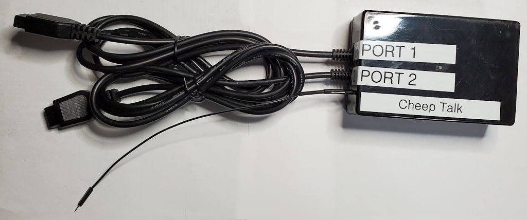
This is the completed Cheep Talk device I built. Requires the use of both joystick ports on the XL/XE computers and being connected to an amplified speaker source. Power for the device is provided by the joystick port(s).
Project Takeaways
I’m quite proud of my work on this project. It turned out fully functional and looks good in the case I had on hand.
- Okay, this has inspired me to dig deeper of the new PCB fabrication being done today. Still like the ferric chloride etching approach but need to up my skills on how we design and prep PCB’s for etching.
- Some may say that what this device does is no different than S.A.M. (Software Automated Mouth), a program for the Atari that does the same thing. However, a key difference is that all the processing for the speech is done on the device allowing the computer to work on the programming more efficiently as it does not need to allocate precious resources to the actual speech processing.
Just a fun project overall even though Amazon Alexa’s speech processing is light years better. Now its on to learning how to program this thing to do more then the sample programs provided in the article.